L3GD20 데이터 시트보기 (PDF) - STMicroelectronics
부품명
상세내역
일치하는 목록
L3GD20 Datasheet PDF : 44 Pages
| |||
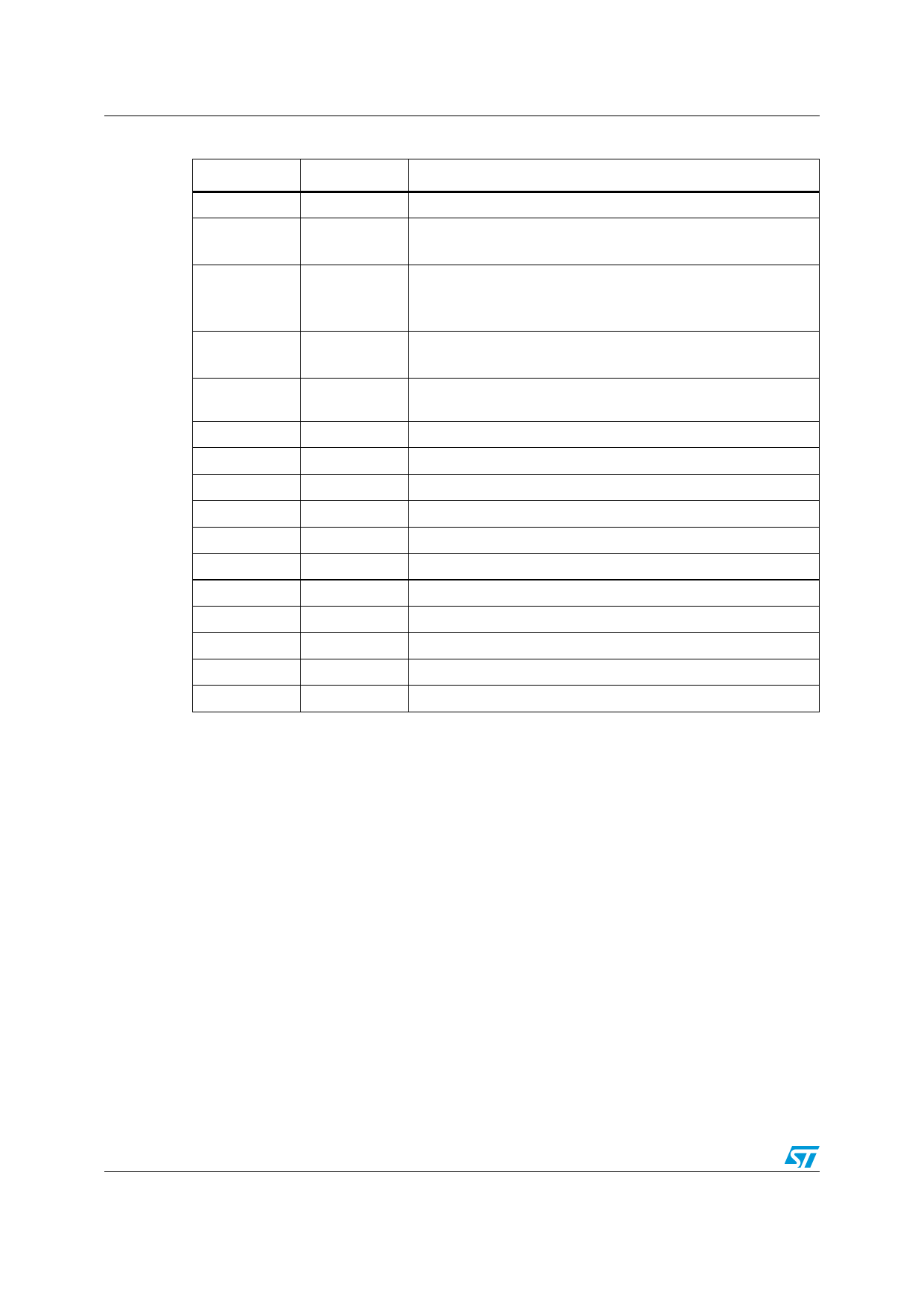
Block diagram and pin description
L3GD20
Table 2. Pin description
Pin#
Name
Function
1
Vdd_IO(1) Power supply for I/O pins
SCL
I2C serial clock (SCL)
2
SPC
SPI serial port clock (SPC)
SDA
I2C serial data (SDA)
3
SDI
SPI serial data input (SDI)
SDO
3-wire interface serial data output (SDO)
SDO
SPI serial data output (SDO)
4
SA0
I2C less significant bit of the device address (SA0)
5
CS
I2C/SPI mode selection (1: SPI idle mode / I2C communication
enabled; 0: SPI communication mode / I2C disabled)
6
DRDY/INT2 Data ready/FIFO interrupt (Watermark/Overrun/Empty)
7
INT1
Programmable interrupt
8
Reserved Connect to GND
9
Reserved Connect to GND
10
Reserved Connect to GND
11
Reserved Connect to GND
12
Reserved Connect to GND
13
GND
0 V supply
14
Reserved Connect to GND with ceramic capacitor(2)
15
Reserved Connect to Vdd
16
Vdd(3)
Power supply
1. 100 nF filter capacitor recommended.
2. 1 nF min value must be guaranteed under 11 V bias condition.
3. 100 nF plus 10 µF capacitors recommended.
8/44
Doc ID 022116 Rev 1
Share Link: 