L3GD20 데이터 시트보기 (PDF) - STMicroelectronics
부품명
상세내역
일치하는 목록
L3GD20 Datasheet PDF : 44 Pages
| |||
L3GD20
Block diagram and pin description
1
Block diagram and pin description
Note:
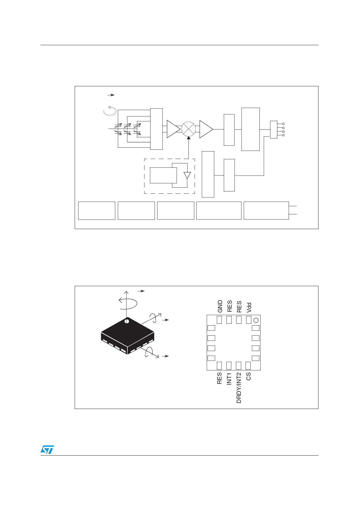
Figure 1. Block diagram
+Ω x,y,z
X+
CHARGE MIXER LOW-PASS
Y+
AMP
FILTER
Z+
M
U
X
Z-
Y-
X-
DRIVING MASS
Feedback loop
T
E
M
P
E
R
A
T
U
S
E
N
S
O
R
R
E
DF
A
D
C
1
I
G
I
T
A
I
L
T
E
R
I
LN
G
A
D
C
2
CS
I2C
SCL/SPC
SPI
SDA/SDO/SDI
SDO
REFERENCE
TRIMMING
CIRCUITS
CLOCK
FIFO
&
PHASE GENERATOR
CONTROL LOGIC
&
INTERRUPT GEN.
INT1
DRDY/INT2
AM10126V1
The vibration of the structure is maintained by drive circuitry in a feedback loop. The sensing
signal is filtered and appears as a digital signal at the output.
1.1
Pin description
Figure 2. Pin connection
+Ω Z
X
+Ω Y
+ ΩX
(TOP VIEW)
DIRECTIONS OF THE
DETECTABLE
ANGULAR RATES
13
16
RES 12
1
RES
RES
BOTTOM
VIEW
Vdd_IO
SCL/SPC
SDA/SDI/SDO
RES 9
8
4 SDO/SA0
5
AM10127V1
Doc ID 022116 Rev 1
7/44
Share Link: 