L3GD20 데이터 시트보기 (PDF) - STMicroelectronics
부품명
상세내역
일치하는 목록
L3GD20 Datasheet PDF : 44 Pages
| |||
Digital main blocks
4
Digital main blocks
L3GD20
4.1
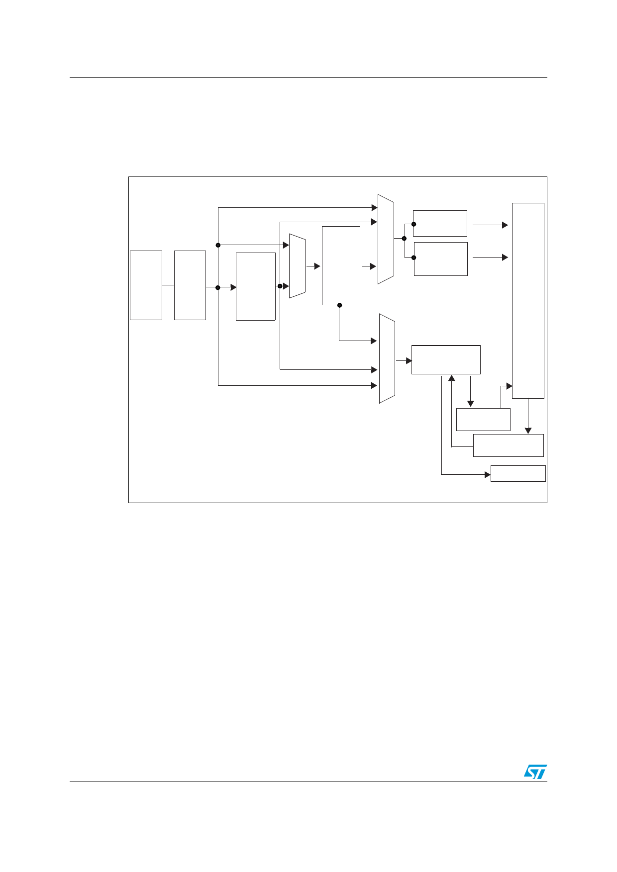
Block diagram
Figure 6. Block diagram
Out_Sel
00
01 DataReg
0
FIFO
LPF2
10
32x16x3
11
ADC LPF1
HPF
1
I2C
SPI
HPen
INT_Sel
10
11
Interrupt
01
generator
00
SCR REG
CONF REG
INT1
AM07230v1
4.2
FIFO
The L3GD20 embeds 32 slots of 16-bit data FIFO for each of the three output channels:
yaw, pitch and roll. This allows consistent power saving for the system, since the host
processor does not need to continuously poll data from the sensor, but can wake up only
when needed and burst the significant data out from the FIFO. This buffer can work
accordingly in five different modes: Bypass mode, FIFO mode, Stream mode, Bypass-to-
Stream mode and Stream-to-FIFO mode. Each mode is selected by the FIFO_MODE bits in
the FIFO_CTRL_REG (2Eh). Programmable Watermark level, FIFO_empty or FIFO_Full
events can be enabled to generate dedicated interrupts on the DRDY/INT2 pin (configured
through CTRL_REG3 (22h) and event detection information is available in FIFO_SRC_REG
(2Fh). Watermark level can be configured to WTM4:0 in FIFO_CTRL_REG (2Eh).
16/44
Doc ID 022116 Rev 1
Share Link: 