NJU6682 데이터 시트보기 (PDF) - Japan Radio Corporation
부품명
상세내역
일치하는 목록
NJU6682 Datasheet PDF : 58 Pages
| |||
NJU6682
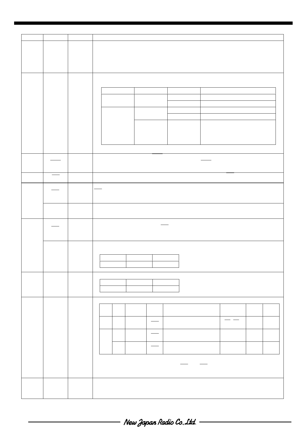
No. Symbol
24
D8
to
to
30
D15
13
A0
8
RES
12
CS
RD
15
(E)
WR
14
(R/W)
7
SEL68
6
PS0
5
PS1
I/O
Function
8-bit Bus Mode & Serial Mode
•Output terminal with Hi-Z status.
I/O
16-bit Bus Mode
•I/O terminals for the upper 8-bits of 16-bit bus.
Normaly, connect to the address bus of MPU. The data on the D0 to D7 is
distinguished as Display Data or Instruction by status of A0.
PS1 terminal PS0 terminal Ao terminal
H
H
L
I
H
H
L
Distinction
Display Data
Instruction
Display Data
Instruction
L
L
The 17th data of serial
data is recognized as A0.
: H or L
Reset terminal. When the RES terminal goes to “L”, the initialization is performed.
I
Reset operation is executing during “L” state of RES.
I
Chip serect terminal. Data Input/Output are available during CS=”L”.
< In case of 80 type MPU ( PS1=”H”, SEL68=”L” ) >
I
RD signal of 80 type MPU input terminal. Active “L”.
During this signal is “L”, D0 to D7 terminals are output.
< In case of 68 type MPU ( PS1=”H”, SEL68=”H” ) >
I
Enable signal of 68 type MPU input terminal. Active “H”.
< In case of 80 type MPU ( PS1=”H”, SEL68=”L” ) >
I
Connect to the 80 type MPU WR signal. Active “L”.
The data on the data bus input syncronizeing the rise edge of this terminal.
< In case of 68 type MPU ( PS1=”H”, SEL68=”H” ) >
The read / Write control signal of 68 type MPU input terminal.
I
R/W
H
L
State
Read
Write
MPU interface type selection terminal.
I
SEL68
H
L
State
68 type 80 type
Serial or parallel type interface selection terminal.
Chip
PS1 PS0 Interface
Select
Data/
Command
Data
Read/ Serial
Write Clock
Write
“H” - Parallel CS
A0
RD WR
-
Only
Serial
Write SCL
I
“H”
CS
A0
4-wire
SI(D7)
Only (D6)
“L”
Serial
The 17th data of serial
Write SCL
“L”
CS
SI(D7)
3-wire
data is recognized as A0.
Only (D6)
10
OSC1
11
OSC2
•In case of serial interface ( PS1=0 ), RD and WR must be fixed to “H” or “L”,
and D0 to D5 will be Hi-Z.
System clock input terminal for Maker testing. ( This terminal should be Open )
I/O
For external clock operation, the clock should be input to OSC1 terminal.
Share Link: 