NJU6682 데이터 시트보기 (PDF) - Japan Radio Corporation
부품명
상세내역
일치하는 목록
NJU6682 Datasheet PDF : 58 Pages
| |||
NJU6682
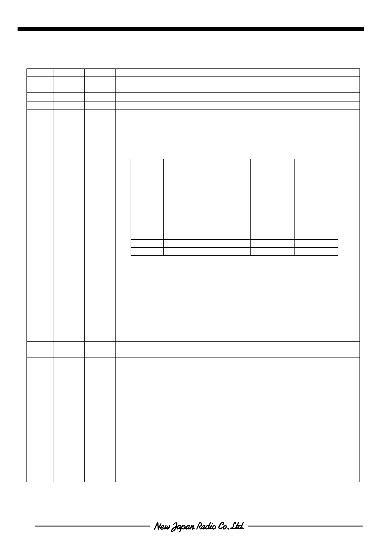
sTERMINAL DESCRIPTION
No. Symbol
2 to 4 DUMMY
1,42,49
9,32
VDD
VSS
I/O
Power
GND
Function
Dummy Terminals.
These terminals are insulated.
2.4V to 3.3V
GND
LCD Driving Voltage Supplying Terminal. When the internal voltage booster is not
used, supply each level of LCD driving voltage from outside with following relation.
VDD≥V1≥V2≥V3≥V4≥V5
When the internal power supply is used, the internal circuits generate and supply
following LCD bias voltage from V1 to V4 terminals.
48
V1
47
V2
46
V3
Power
45
V4
44
V5
Bias
1/4Bias
1/5Bias
1/6Bias
1/7Bias
1/8Bias
1/9Bias
1/10Bias
1/11Bias
1/12Bias
1/13Bias
1/14Bias
V1
V5+3/4Vlcd
V5+4/5Vlcd
V5+5/6Vlcd
V5+6/7Vlcd
V5+7/8Vlcd
V5+8/9Vlcd
V5+9/10Vlcd
V5+10/11Vlcd
V5+11/12Vlcd
V5+12/13Vlcd
V5+13/14Vlcd
V2
V5+2/4Vlcd
V5+3/5Vlcd
V5+4/6Vlcd
V5+5/7Vlcd
V5+6/8Vlcd
V5+7/9Vlcd
V5+8/10Vlcd
V5+9/11Vlcd
V5+10/12Vlcd
V5+11/13Vlcd
V5+12/14Vlcd
V3
V5+2/4Vlcd
V5+2/5Vlcd
V5+2/6Vlcd
V5+2/7Vlcd
V5+2/8Vlcd
V5+2/9Vlcd
V5+2/10Vlcd
V5+2/11Vlcd
V5+2/12Vlcd
V5+2/13Vlcd
V5+2/14Vlcd
V4
V5+1/4Vlcd
V5+1/5Vlcd
V5+1/6Vlcd
V5+1/7Vlcd
V5+1/8Vlcd
V5+1/9Vlcd
V5+1/10Vlcd
V5+1/11Vlcd
V5+1/12Vlcd
V5+1/13Vlcd
V5+1/14Vlcd
(Vlcd=Vdd-V5)
41
C1+
40
C1-
39
C2+
38
C2-
37
C3-
36
C4-
35
C5-
34
C6-
Step up capacitor connecting terminals.
O
Voltage booster circuit ( adjustable with 2 to 7 times )
33
VOUT
43
VR
16
D0
to
to
23
D7
(23)
(SI)
(22)
(SCL)
Step up voltage output terminal. Connect the step up capacitor between this terminal
O
and VSS.
I
Voltage adjust terminal. V5 level is adjusted by external bleeder resistance connecting
between VDD and V5 terminal.
( P/S="H" )In Pararel Interface Mode
•8-bit bus mode*1: I/O terminals for 8-bit bus.
•16-bit bus mode*1: I/O terminals for the 8-bits of lower ranks of 16-bit bus.
*1 To set these 8-bit / 16-bit mode, use Instruction ” 8-bit / 16-bit Bus
Select ”.
I/O
( P/S="L" )In Serial Interface Mode
•D7: Input terminal for serial data ( SI ).
•D6: Input terminal for serial data clock ( SCL ).
When select these mode, D0 to D5 will be Hi-Z status.
( CS=”H” ) D0 to D7 shown Hi-Z.
Share Link: 