AD766 데이터 시트보기 (PDF) - Analog Devices
부품명
상세내역
일치하는 목록
AD766 Datasheet PDF : 8 Pages
| |||
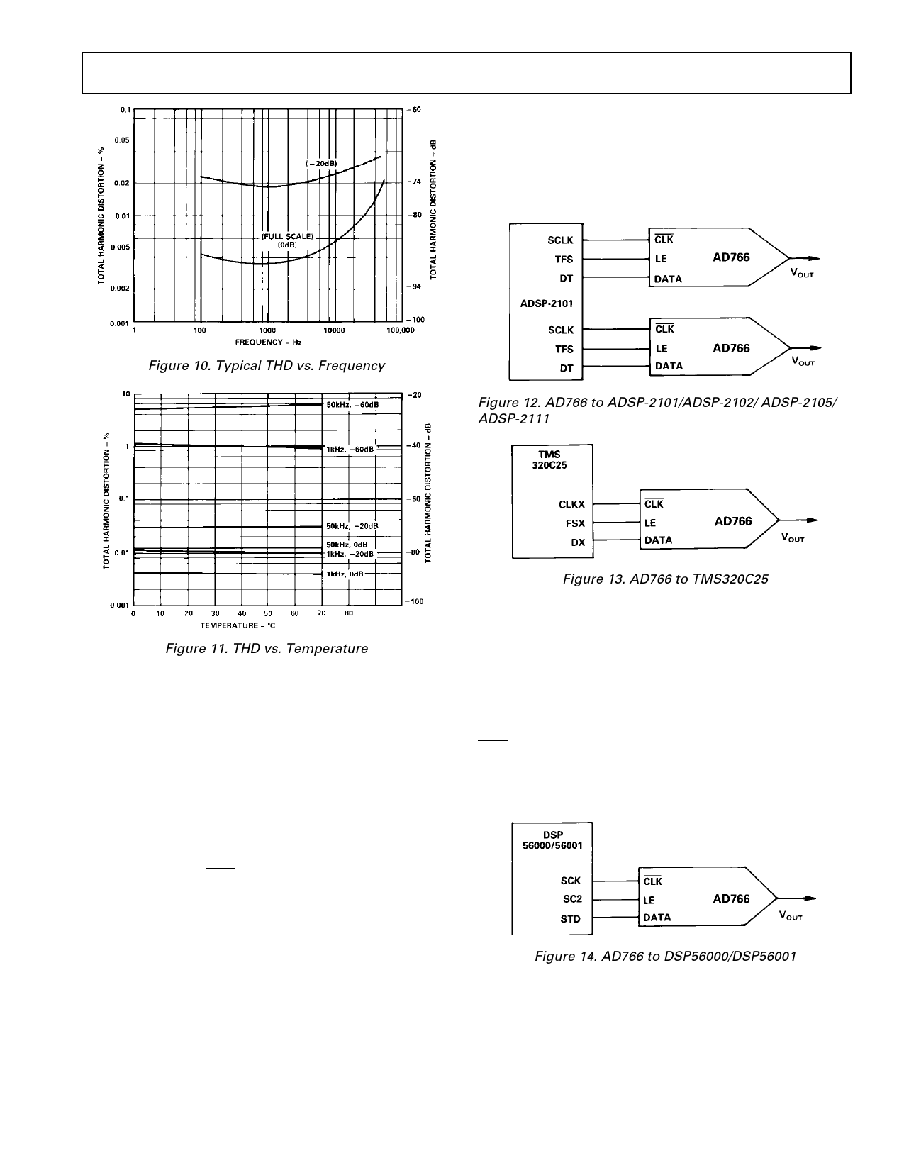
Applications–AD766
AD766 TO TMS320C25
Figure 13 shows the zero-chip interface to the TMS320C25.
The interface to other TMS320C2X processors is similar. Note
that the C25 should be run in continuous mode. The C25’s
frame synch signal (FSX) will be asserted at the beginning of
each 16-bit word but will actually latch in the previous word.
Figure 10. Typical THD vs. Frequency
Figure 12. AD766 to ADSP-2101/ADSP-2102/ ADSP-2105/
ADSP-2111
Figure 11. THD vs. Temperature
INTERFACING THE AD766 TO DIGITAL SIGNAL
PROCESSORS
The AD766 is specifically designed to easily interface to several
popular digital signal processors (DSP) without any additional
logic. Such an interface reduces the possibility of interface prob-
lems and improves system reliability by minimizing component
count.
AD766 TO ADSP-2101
The ADSP-2101 incorporates two complete serial ports which
can be directly interfaced to the AD766 as shown in Figure 12.
The SCLK, TFS and DT outputs of the ADSP-2101 are con-
nected directly to the CLK, LE and DATA inputs of the
AD766, respectively. SCLK is internally generated and can be
programmed to operate from 94 Hz to 6.25 MHz. Data (DT) is
valid on the falling edge of SCLK. After 16 bits have been trans-
mitted, the falling edge of TFS updates the AD766’s data latch.
Using both serial ports of the ADSP-2101, two AD766’s can be
directly interfaced with no additional hardware.
Figure 13. AD766 to TMS320C25
The CLKS, FSX and DX outputs of the TMS320C25 are con-
nected to the CLK, LE and DATA inputs of the AD766, re-
spectively. Data (DX) is valid on the falling edge of CLKX. The
maximum serial clock rate of the TMS320C25 is 5 MHz.
AD766 TO DSP56000/56001
Figure 14 shows the zero-chip interface to the DSP56000/
56001. The SSI of the 56000/56001 allows serial clock rates up
to fosc/4. SCK, SC2 and STD can be directly connected to the
CLK, LE and DATA inputs of the AD766. The CRA control
register of the 56000 allows SCK to be internally generated and
software configurable to various divisions of the master clock
frequency. The data (STD) is valid on the falling edge of SCK.
Figure 14. AD766 to DSP56000/DSP56001
REV. A
–7–
Share Link: 