AD766 데이터 시트보기 (PDF) - Analog Devices
부품명
상세내역
일치하는 목록
AD766 Datasheet PDF : 8 Pages
| |||
Analog Circuit Considerations–AD766
For applications requiring broader bandwidths and/or even
lower noise than that afforded by the AD766’s internal op amp,
an external op amp can easily by used in its place. IOUT (Pin 13)
drives the negative (inverting) input terminal of the external op
amp, and its external voltage output is connected to the feed-
back resistor pin, RF (Pin 10). To insure that the AD766’s un-
used internal op amp remains in a closed-loop configuration,
VOUT (Pin 9) should be tied to the summing junction pin, SJ
(Pin 11).
As an example, Figure 3 shows the AD766 using the AD744 op
amp as an external current-to-voltage converter. In this invert-
ing configuration, the AD744 will provide the same ± 3 V out-
put as the internal op amp would have. Other recommended
amplifiers include the AD845 and AD846. Note that a single
pole of low-pass filtering could also be attained with this circuit
simply by adding a capacitor in parallel with the feedback resis-
tor as just shown in Figure 1.
Figure 3. External Op Amp Connections
Residual DAC differential linearity error around midscale can
be externally trimmed out, improving THD beyond the
AD766’s guaranteed tested specifications. This error is most
significant with low-amplitude signals because the ratio of the
midscale linearity error to the signal amplitude is greatest in this
case, thereby increasing THD. The MSB adjust circuitry shown
in Figure 4 can be used for improving THD with low-level sig-
nals. Otherwise, the AD766 will operate to its specifications
with MSB ADJ (Pin 14) and TRIM (Pin 15) unconnected.
Figure 4. Optional MSB Adjustment Circuit
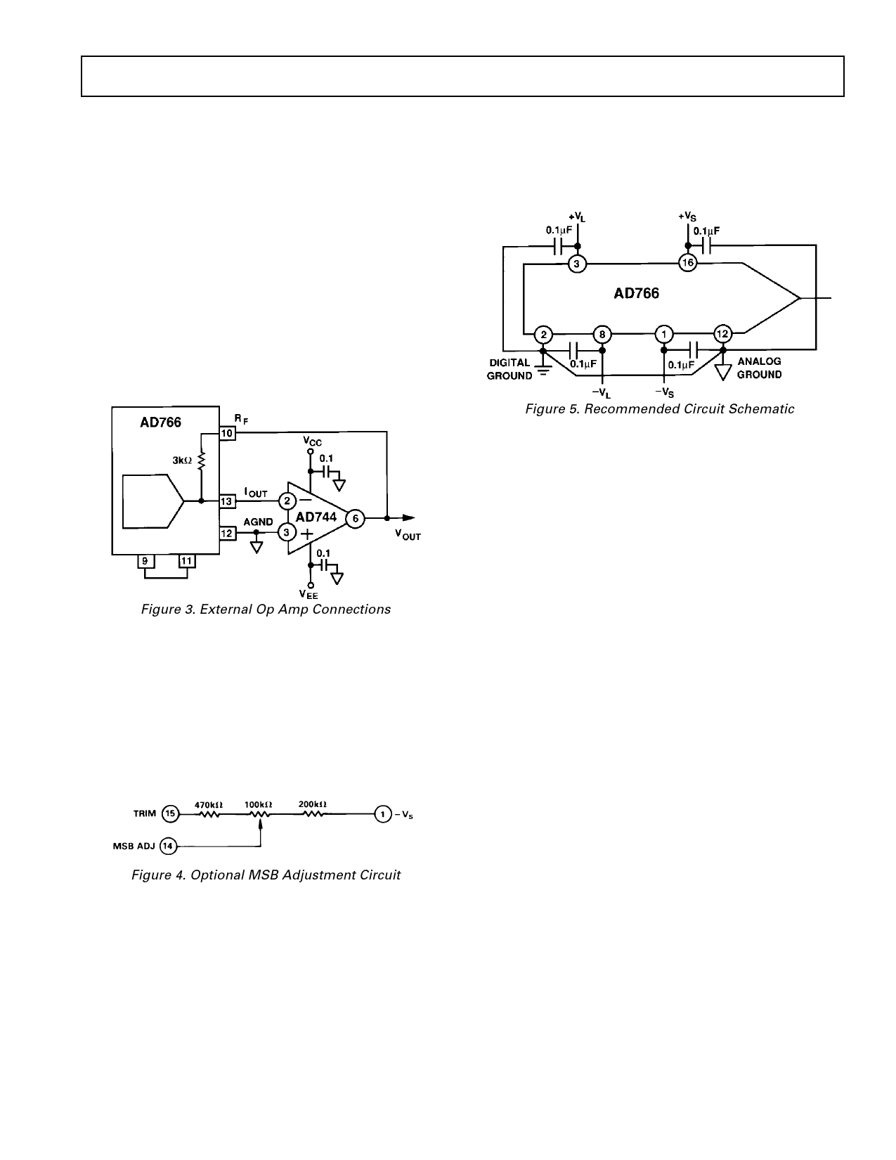
ANALOG CIRCUIT CONSIDERATIONS
GROUNDING RECOMMENDATIONS
The AD766 has two ground pins, designated AGND (analog
ground) and DGND (digital ground). The analog ground pin is
the “high-quality” ground reference point for the device. The
analog ground pin should be connected to the analog common
point in the system. The output load should also be connected
to that same point.
The digital ground pin returns ground current from the digital
logic portions of the AD766 circuitry. This pin should be con-
nected to the digital common point in the system.
As illustrated in Figure 5, the analog and digital grounds should
be connected together at one point in the system.
Figure 5. Recommended Circuit Schematic
POWER SUPPLIES AND DECOUPLING
The AD766 has four power supply input pins. ± VS provide the
supply voltages to operate the linear portions of the DAC in-
cluding the voltage reference, output amplifier and control am-
plifier. The ± VS supplies are designed to operate from ± 5 V to
± 12 V.
The ± VL supplies operate the digital portions of the chip, in-
cluding the input shift register and the input latching circuitry.
The ± VL supplies are also designed to operate from ± 5 V to
± 12 V. To assure freedom from latch-up, –VL should never go
more negative than –VS.
Special restrictions on power supplies apply to extended tem-
perature range versions of the AD766 that do not apply to the
commercial AD766J. First, supplies must be symmetric. That is,
+VS = ͉–VS͉ and +VL = ͉–VL͉. Each supply must independently
meet this equality within ± 5%. Since we require that –VS ≤ –VL
to guarantee latch-up immunity, this symmetry principle implies
that the positive analog supply must be greater than or equal to
the positive digital supply, i.e., VS ≥ –VL for extended-temper-
ature range parts. In other words, the digital supply range must
be inside the analog supply range. Second, the internal op amp’s
performance in generating voltage outputs is only guaranteed if
+VS ≥ 7 V (and –VS ≤ –7 V, by the symmetry principle). These
constraints do not apply to the AD766J.
Decoupling capacitors should be used on all power supply pins.
Furthermore, good engineering practice suggests that these ca-
pacitors be placed as close as possible to the package pins as
well as the common points. The logic supplies, ± VL, should be
decoupled to digital common; and the analog supplies, ± VS,
should be decoupled to analog common.
The use of four separate power supplies will reduce feedthrough
from the digital portion of the system to the linear portions of
the system, thus contributing to the performance as tested.
However, four separate voltage supplies are not necessary for
good circuit performance. For example, Figure 6 illustrates a
REV. A
–5–
Share Link: 