MC74HCT541AN 데이터 시트보기 (PDF) - ON Semiconductor
부품명
상세내역
일치하는 목록
MC74HCT541AN
ON Semiconductor

MC74HCT541AN Datasheet PDF : 8 Pages
| |||
MC74HCT541A
PIN DESCRIPTIONS
INPUTS
A1, A2, A3, A4, A5, A6, A7, A8 (PINS 2, 3, 4, 5, 6, 7, 8,
9) — Data input pins. Data on these pins appear in
non–inverted form on the corresponding Y outputs, when
the outputs are enabled.
CONTROLS
OE1, OE2 (PINS 1, 19) — Output enables (active–low).
When a low voltage is applied to both of these pins, the
outputs are enabled and the device functions as a
non–inverting buffer. When a high voltage is applied to
either input, the outputs assume the high impedance state.
OUTPUTS
Y1, Y2, Y3, Y4, Y5, Y6, Y7, Y8 (PINS 18, 17, 16, 15, 14,
13, 12, 11) — Device outputs. Depending upon the state of
the output enable pins, these outputs are either
non–inverting outputs or high–impedance outputs.
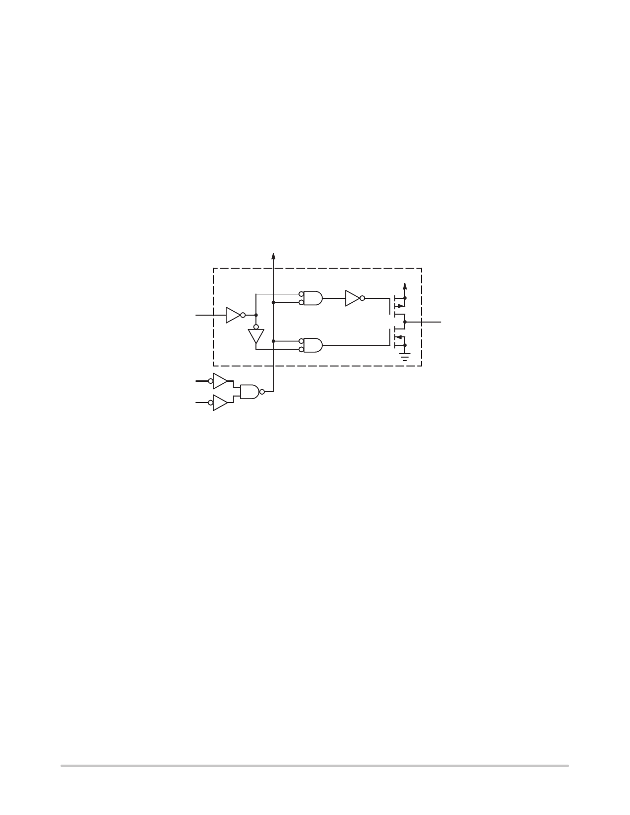
LOGIC DETAIL
To 7 Other
Buffers
INPUT A
One of Eight
Buffers
VCC
OUTPUT Y
OE1
OE2
http://onsemi.com
4
Share Link: