MC74HCT541AN 데이터 시트보기 (PDF) - ON Semiconductor
부품명
상세내역
일치하는 목록
MC74HCT541AN
ON Semiconductor

MC74HCT541AN Datasheet PDF : 8 Pages
| |||
MC74HCT541A
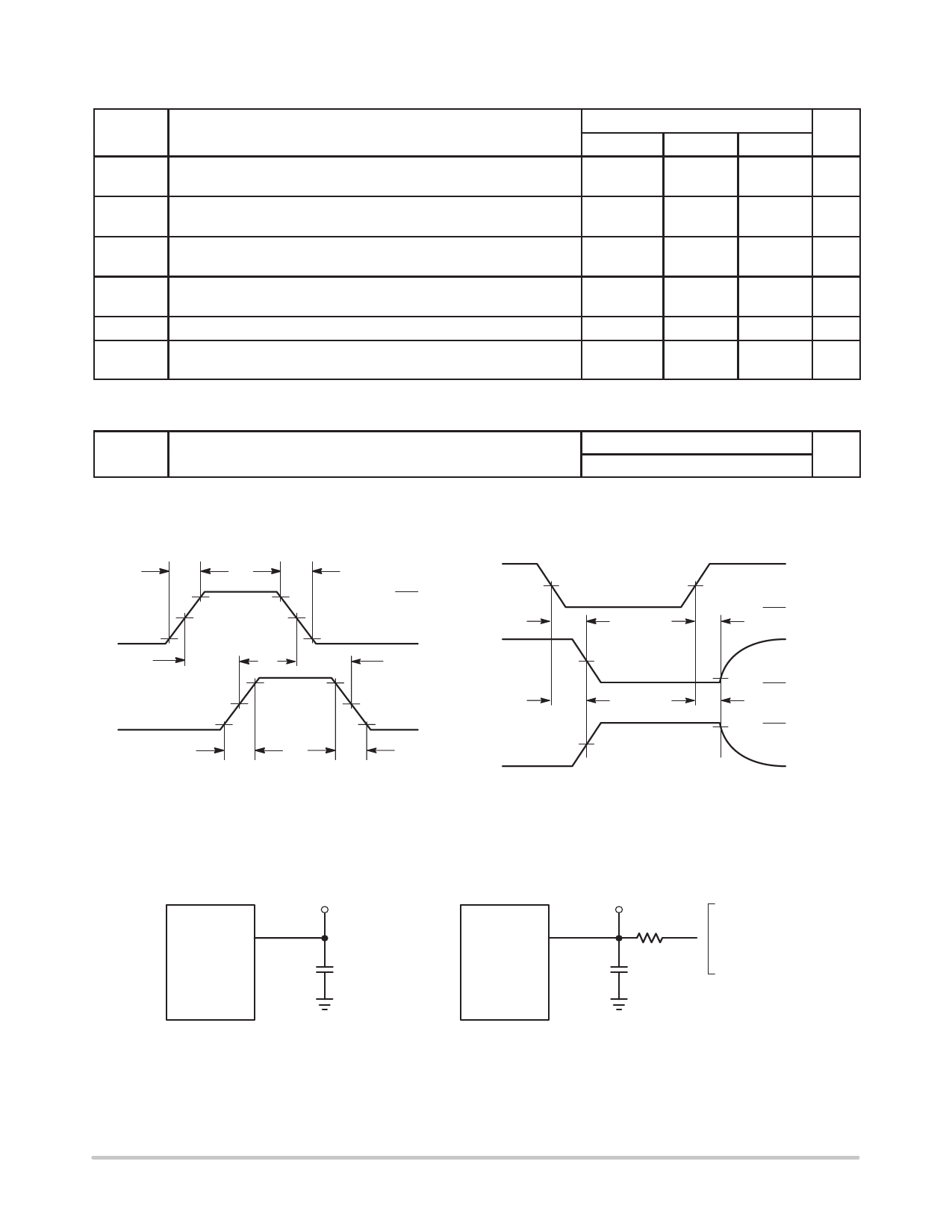
AC CHARACTERISTICS (VCC = 5.0V, CL = 50 pF, Input tr = tf = 6 ns)
Symbol
Parameter
Guaranteed Limit
–55 to 25°C ≤85°C
≤125°C Unit
tPLH,
Maximum Propagation Delay, Input A to Output Y
23
tPHL
(Figures 1 and 3)
tPLZ,
Maximum Propagation Delay, Output Enable to Output Y
30
tPHZ
(Figures 2 and 4)
tPZL,
Maximum Propagation Delay, Output Enable to Output Y
30
tPZH
(Figures 2 and 4)
tTLH,
Maximum Output Transition Time, Any Output
12
tTHL
(Figures 1 and 3)
Cin
Maximum Input Capacitance
10
Cout
Maximum Three–State Output Capacitance (Output in High Impedance
15
State)
28
32
ns
34
38
ns
34
38
ns
15
18
ns
10
10
pF
15
15
pF
NOTE: For propagation delays with loads other than 50 pF, and information on typical parametric values, see Chapter 2 of the ON
Semiconductor High–Speed CMOS Data Book (DL129/D).
Typical @ 25°C, VCC = 5.0 V
CPD Power Dissipation Capacitance (Per Buffer)*
55
pF
* Used to determine the no–load dynamic power consumption: PD = CPD VCC2f + ICC VCC. For load considerations, see Chapter 2 of the
ON Semiconductor High–Speed CMOS Data Book (DL129/D).
SWITCHING WAVEFORMS
tr
INPUT A
tPLH
90%
1.3V
10%
90%
OUTPUT Y
1.3V
10%
tTLH
tf
OE1 or OE2
3.0V
GND
tPHL
OUTPUT Y
OUTPUT Y
tTHL
Figure 1.
1.3V
tPZL tPLZ
1.3V
tPZH tPHZ
1.3V
1.3V
10%
90%
Figure 2.
3.0V
GND
HIGH
IMPEDANCE
VOL
VOH
HIGH
IMPEDANCE
TEST CIRCUITS
DEVICE
UNDER
TEST
TEST
POINT
OUTPUT
CL*
DEVICE
UNDER
TEST
TEST
POINT
OUTPUT
1kΩ
CL*
CONNECT TO VCC WHEN
TESTING tPLZ AND tPZL.
CONNECT TO GND WHEN
TESTING tPHZ and tPZH.
*Includes all probe and jig capacitance
Figure 3.
*Includes all probe and jig capacitance
Figure 4.
http://onsemi.com
3
Share Link: