MC143416PB 데이터 시트보기 (PDF) - Freescale Semiconductor
부품명
상세내역
일치하는 목록
MC143416PB Datasheet PDF : 24 Pages
| |||
Freescale Semiconductor, Inc.
REGISTER PROGRAMMING
REGISTER PROGRAMMING MODEL
Table 6 is the register map of the MC143416’s control and
status registers. Registers labeled with a 0 suffix are
associated with SSI Port 0, and those with a 1 suffix are
associated with SSI Port 1. For example, register CNTL0_0
is associated with SSI Port 0, and CNTL0_1 is associated
with SSI Port 1.
CONTROL AND STATUS REGISTERS
The MC143416 provides ten 8–bit control/status registers
that are available to use. The MSB of all these registers is
always 0 as a safety feature against desynchronization (ad-
dress/data swap). Each register is doubled to serve one
associated codec, with the exception of register CNTL4,
CNTL5, CNTL6, and CNTL7, which carry global chip con-
trols. These registers are accessible by either SSI port.
In the following paragraphs, the contents of each register
are discussed in detail. In the description of each individual
bit, two parameters are included: access and reset value. Ac-
cess indicates whether the bit is read only, write only, or both;
reset value indicates the value upon reset. All register bits
are static except SWRESET in CNTL4.
CNTL0_0: Power Control Register — Codec 0
ANARSVD0 (R/W, 0): This bit is reserved for future use
and must be kept 0.
ALOOP (R/W, 0): This bit controls the remote loopback
function at the analog/digital interface. Setting this bit to 1 will
force the single bit modulated output from Rx in the codec to
loopback into the single bit input of the D/A. See Figure 4.
DLOOP (R/W, 0): Setting this bit to 1 will force a digital
loopback in the codec. This occurs at a point between the
output of digital interpolator filter and the input of the digital
decimator filter. See Figure 4.
RST (R/W, 1): Setting this bit to 1 will force a value of 0x00
to all digital processing stages.
PWDN (R/W, 1): Setting this bit to 1 will disable all data
processing for this codec and power down the associated
analog circuitry.
TxEN (R/W, 0): Setting this bit to 1 will enable the trans-
mitter on the codec. The transmitter is a differential mode
power stage. When disabled, the amplifier maintains a zero
differential output voltage (AO0+ = AO0– = VAG).
ALOCAL LOOP (R/W, 0): As opposed to the ALOOP bit of
this register, ALOCAL LOOP closes a local loopback at the
analog interface. When this bit is set active (1), the analog
output signal on pins AO0+ and AO0– is fed back into the in-
put amplifier stage on pins AI0+ and AI0–. See Figure 4.
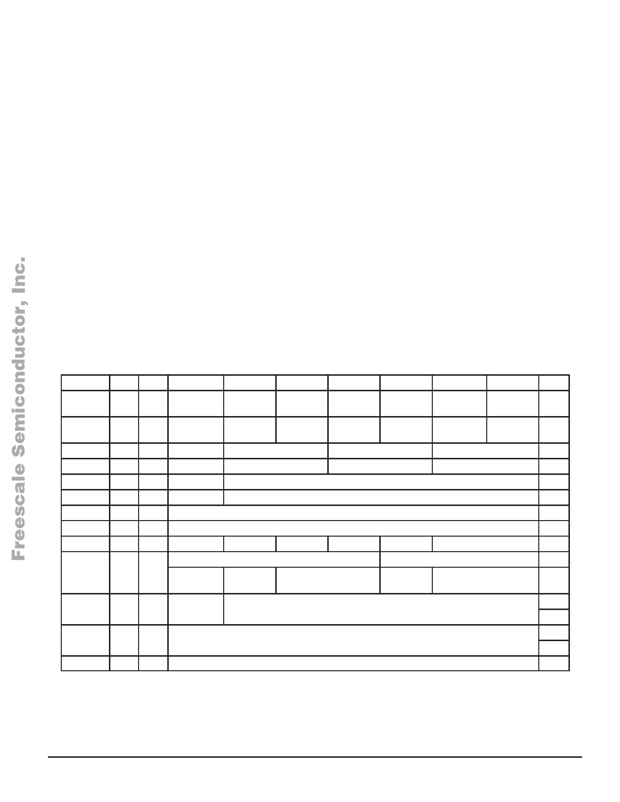
Table 6. Register Map
Register Addr 7
6
5
4
3
2
1
0
Mode
CNTL0_0 0x0
0 ANARSVD0 ALOOP0 DLOOP0
PWDN0
RST0
TxEN0
ALOCAL R/W
LOOP
CNTL0_1 0x1 0 ANARSVD1 ALOOP1 DLOOP1 PWDN1
RST1
TxEN1
ALOCAL R/W
LOOP
CNTL1_0 0x2
0
HPF_EN0
IN_GAIN0(1:0)
SPK_Rx0(1:0)
SPK_Tx0(1:0)
R/W
CNTL1_1 0x3
CNTL2_0 0x4
0
HPF_EN1
0 MCLK0_SEL
IN_GAIN1(1:0)
SPK_Rx1(1:0)
HSDIV0(5:0)
SPK_Tx1(1:0)
R/W
R/W
CNTL2_1 0x5 0 MCLK1_SEL
HSDIV1(5:0)
R/W
CNTL3_0 0x6 0
LSDIV0(6:0)
R/W
CNTL3_1 0x7 0
LSDIV1(6:0)
R/W
CNTL4 0x8 0
CNTL5 0x9 0
SWRESET RSVD
SSI_SEL
SYS_DIV(1:0)
R/W
SELF_CHECK (2:0)
RO
TEST_RSVD (1:0)
SERIAL
LOOP
TEST_MODE (1:0)
WO
CNTL6
0
CNTL7
0
WO
RSVD (5:0)
RO
WO
RSVD (6:0)
RO
SYNC 0xF 0
SEE DESCRIPTION
R/W
MOTOROLA
For More Information On This Product,
Go to: www.freescale.com
MC143416
11
Share Link: 