MAX17491 데이터 시트보기 (PDF) - Maxim Integrated
부품명
상세내역
일치하는 목록
MAX17491 Datasheet PDF : 12 Pages
| |||
Single-Phase Synchronous MOSFET Driver
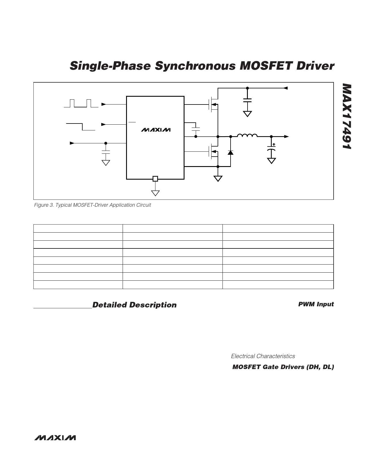
PWM SKIP
+5V BIAS
SUPPLY
CVDD
1.0μF
PWM
DH
SKIP
BST
MAX17491 LX
VDD
DL
GND
PAD
NH
CBST
0.22μF
CIN
2x 10μF
L1
0.36μH
NL
DL
INPUT (VIN)
OUTPUT (VOUT)
COUT
2x 330μF
6mΩ
Figure 3. Typical MOSFET-Driver Application Circuit
Table 1. Typical Components
DESIGNATION
NH
NL
BST Capacitor (CBST)
Schottky Diode
Inductor (L1)
Output Capacitors (COUT)
Input Capacitors (CIN)
QTY
1 per phase
1–2 per phase
1 per phase
Optional
1 per phase
1–2 per phase
1–2 per phase
COMPONENT SUPPLIERS
Siliconix Si4860DY
Siliconix Si4336DY
0.1µF or 0.22µF ceramic capacitor
3A, 40V Schottky diode
0.36µH, 26A, 0.9mΩ power inductor
330µF, 6mΩ per phase
10µF, 25V X5R ceramic capacitors
Detailed Description
The MAX17491 single-phase gate driver, along with the
MAX8736, MAX8786, or MAX17030 multiphase con-
trollers, provide flexible multiphase CPU core-voltage
supplies. The low driver resistance allows up to 7A out-
put peak current. Each MOSFET driver in the
MAX17491 can drive 3nF capacitive loads with only 9ns
propagation delay and 4ns/8ns (typ) fall/rise times,
allowing operation up to 3MHz per phase. Larger
capacitive loads are allowable but result in longer prop-
agation and transition times. Adaptive dead-time con-
trol prevents shoot-through currents and maximizes
converter efficiency while allowing operation with a vari-
ety of MOSFETs and PWM controllers. An input under-
voltage-lockout (UVLO) circuit allows proper power-on
sequencing.
PWM Input
The drivers for the MAX17491 are disabled—DH and
DL pulled low—if the PWM input remains in the midlevel
window for at least 300ns (typ). Once the PWM signal is
driven high or low, the MAX17491 immediately exits the
low-current shutdown state and resumes active opera-
tion. Outside the shutdown state, the drivers are
enabled based on the rising and falling thresholds
specified in the Electrical Characteristics.
MOSFET Gate Drivers (DH, DL)
The high-side driver (DH) has a 0.9Ω sourcing resis-
tance and 0.7Ω sinking resistance, resulting in 2.2A
peak sourcing current and 2.7A peak sinking current
with a 5V supply voltage. The low-side driver (DL) has a
typical 0.7Ω sourcing resistance and 0.3Ω sinking
resistance, yielding 2.7A peak sourcing current and 8A
peak sinking current. This reduces switching losses,
making the MAX17491 ideal for both high-frequency
and high-output-current applications.
_______________________________________________________________________________________ 7
Share Link: 