JBT6K49-AS 데이터 시트보기 (PDF) - Toshiba
부품명
상세내역
일치하는 목록
JBT6K49-AS Datasheet PDF : 14 Pages
| |||
JBT6K49-AS
Description of Functions and Operation
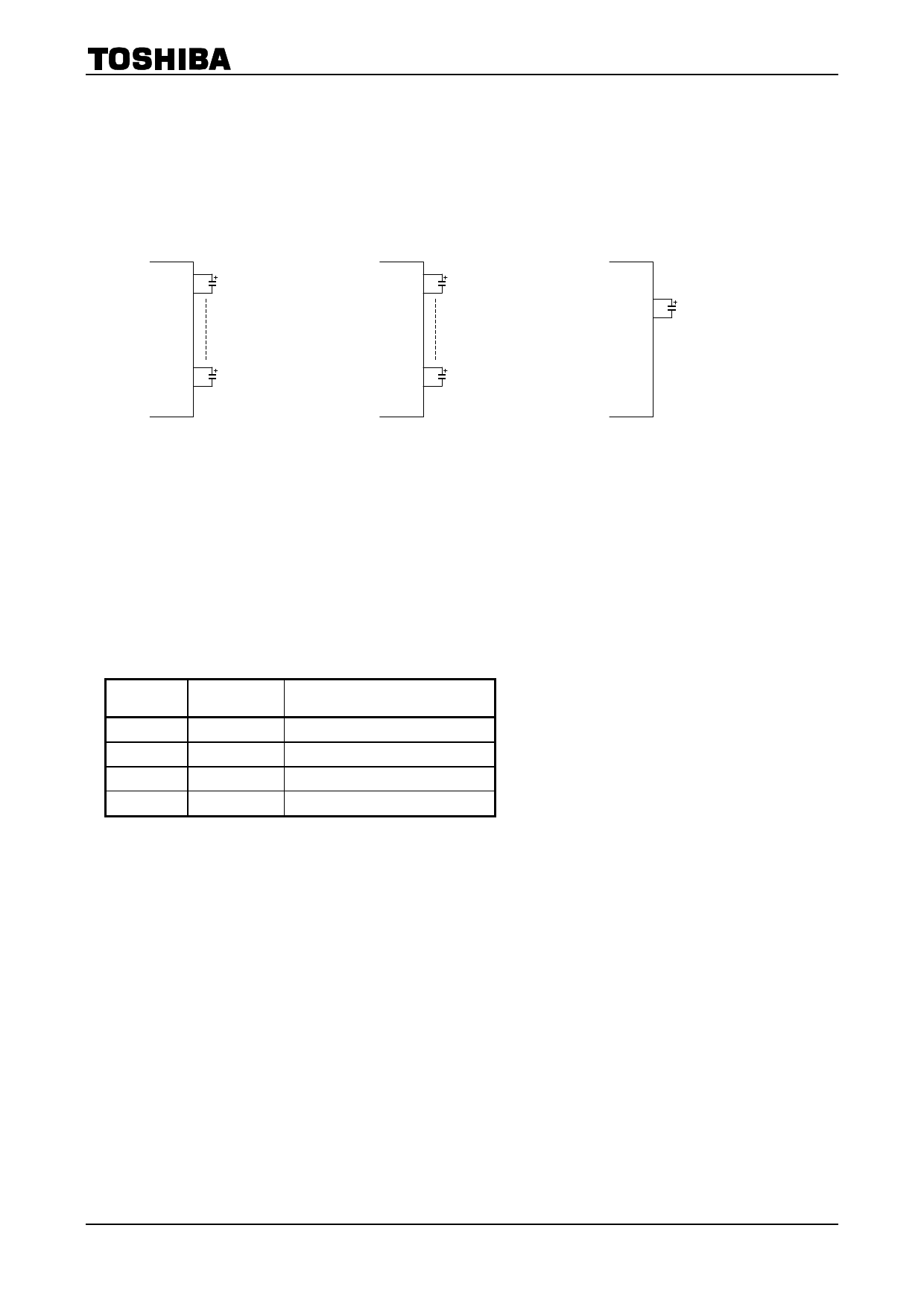
DC-DC converter
The JBT6K49-AS generates an analog supply voltage for the source driver (T6K47) and an LCD-driving
voltage for the gate driver (T6K48). The DC-DC converter consists of three circuit blocks which output +4.8 V,
+13.0 V and -13.0 V. The ways in which the DC-DC converter can be used are shown below.
DC-DC converter (1):
Generates +4.8 V.
CA1 +
CA1 -
DC-DC converter (1):
Generates +13.0 V.
CB1 +
CB1 -
DC-DC converter (1):
Generates -13.0 V.
CC1 +
CC1 -
CA2 +
CA2 -
CB5 +
CB5 -
Note 2:
Connect a voltage boosting kick capacitor or capacitors to each circuit block. Normally the capacitance of
the kick capacitor should be 1.0 mF. Connect a 10 mF capacitor across the boosted-voltage output pin and
the VSS pin of DC-DC converter (1), since the voltage generated in the DC-DC converter is unstable. In
addition, connect a 1 mF capacitor across the boosted-voltage output pin and the VSS pin of DC-DC
converter (1).
Oscillation Circuit
The JBT6K49-AS generates the clock pulse used by the DC-DC converter. The FSEL1 and FSEL2 pins can be
used to select the clock oscillation frequency. The following table lists the correspondence between the pin
settings and the selected frequency.
FSEL2
FSEL1
Oscillation Frequency (initial value)
0
0
0
1
1
0
1
1
3.5 kHz
5.0 kHz
7.0 kHz
10.0 kHz
Note 3: The relationship of the oscillation frequency and the oscillation resistance depends on assembly and
measuring conditions.
Therefore, select the oscillation resistance after enough evaluating.
9
2002-03-12
Share Link: 