JBT6K49-AS 데이터 시트보기 (PDF) - Toshiba
부품명
상세내역
일치하는 목록
JBT6K49-AS Datasheet PDF : 14 Pages
| |||
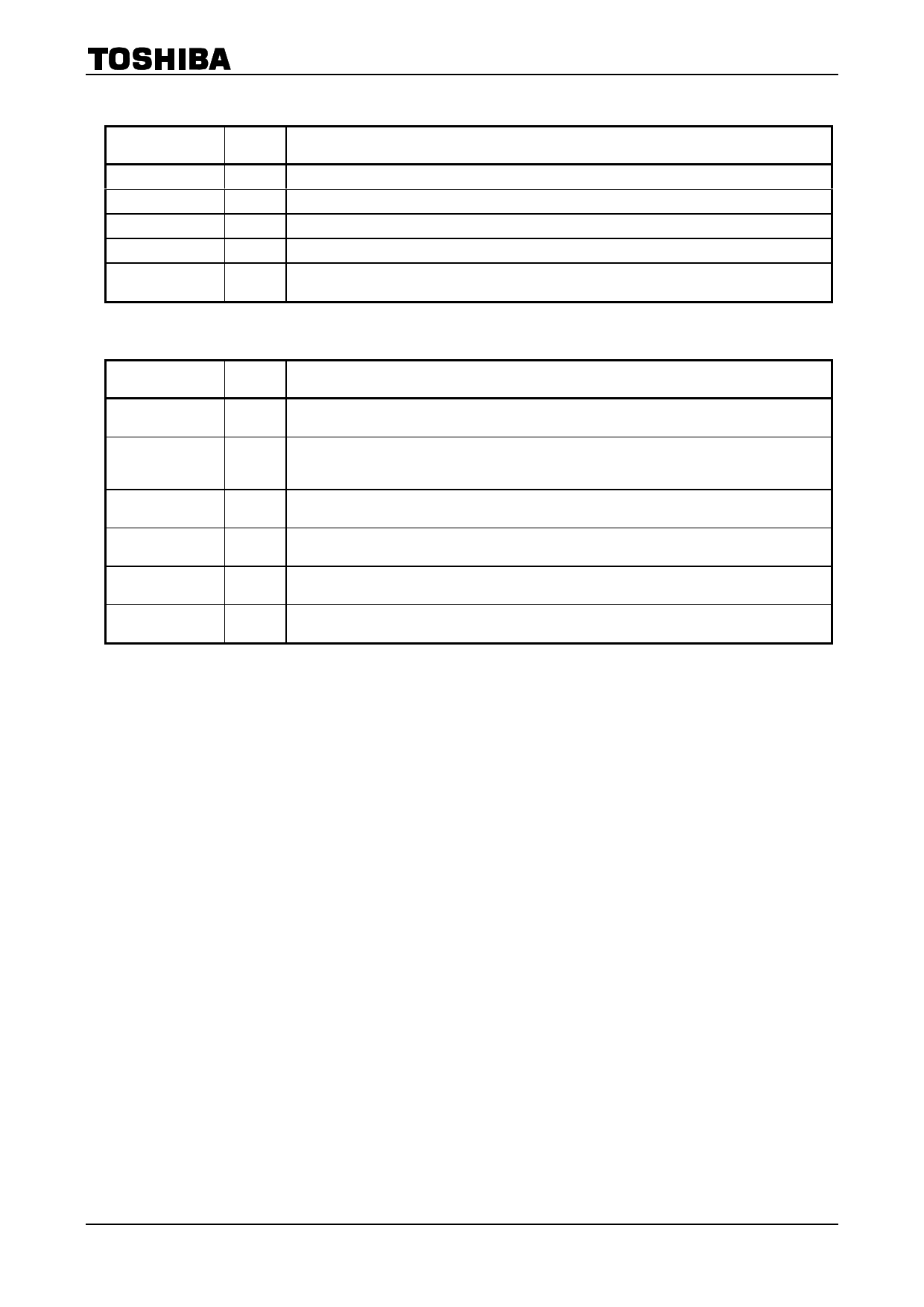
Pin Function Description (3)
JBT6K49-AS
Pin Name
VBAT
VDD
VCC
VEE
GND1、GND2
I/O
Function
¾ Analog circuit supply voltage
¾ Logic circuit supply voltage
¾ DC-DC converter 2 supply voltage
¾ DC-DC converter 3 supply voltage
¾ Ground pins
Note 2: The GND1 and GND2 pins serve different circuit blocks. Connect both pins to ground.
Pin Function Description (4)
Pin Name
TEST
SCK
SDA
FUSE**
FUSE*G
TEG**
I/O
Function
I
Test mode switching pin
This is an enable pin for Toshiba Test Mode. Normally it should be grounded.
I
Test mode clock pin
A clock pulse for serial data transfer used in Toshiba Test Mode is input on this pin. Normally it
should be grounded.
I
Test mode data pin
Serial data used in Toshiba Test Mode is input on this pin. Normally it should be grounded.
I
Toshiba test pin (1)
This pin is a dedicated pin used only in Toshiba Test Mode. Normally it should be left open.
I
Toshiba test pin (2)
This pin is a dedicated pin used only in Toshiba Test Mode. Normally it should be left open.
I
Toshiba test pin (3)
This pin is a dedicated pin used only in Toshiba Test Mode. Normally it should be left open.
8
2002-03-12
Share Link: 