ICS9147-01 데이터 시트보기 (PDF) - Integrated Device Technology
부품명
상세내역
일치하는 목록
ICS9147-01 Datasheet PDF : 11 Pages
| |||
ICS9147- 01
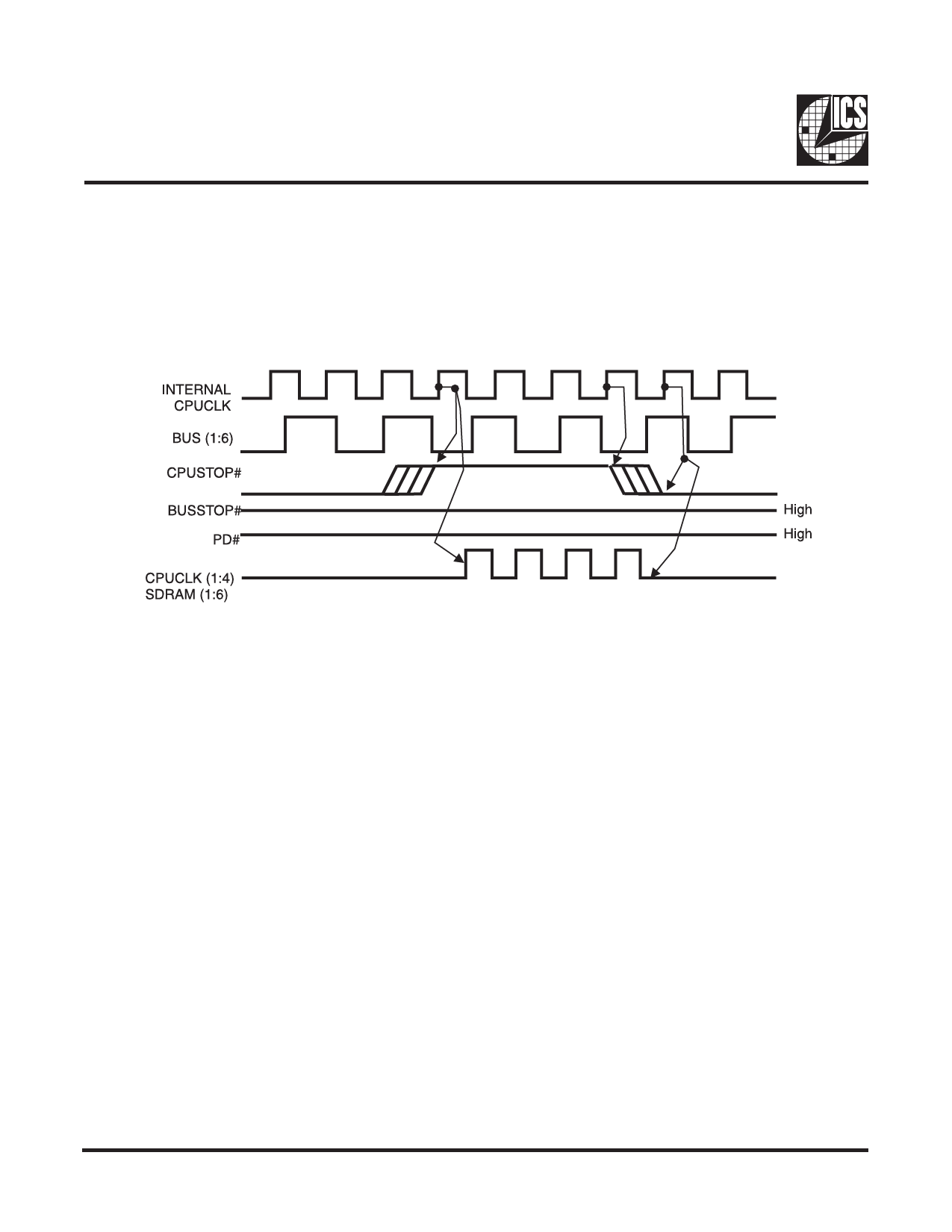
CPUSTOP# Timing Diagram
CPUSTOP# is an asychronous input to the clock synthesizer. It is used to turn off the CPU clocks for low power operation.
CPUSTOP# is synchronized by the ICS9147-01. All other clocks will continue to run while the CPU and SDRAM clocks
are disabled. The CPU and SDRAM clocks will always be stopped in a low state and start in such a manner that guarantees
the high pulse width is a full pulse. CPU clock on latency is 0 to 1 CPU clocks and CPU clock off latency is 0 to 1 CPU
clocks.
Notes:
1. All timing is referenced to the internal CPU clock.
2. CPUSTOP# is an asynchronous input and metastable conditions
may exist. This signal is synchronized to the CPU and SDRAM
clocks inside the ICS9147-01.
3. All other clocks continue to run undisturbed.
4. PD# and BUSSTOP# are shown in a high (true) state.
BUSSTOP#Timing Diagram
BUSSTOP# is an asynchronous input to the ICS9147-01. It is used to turn off the BUS (1:6) clocks for low power operation.
BUSSTOP# is synchronized by the ICS9147-01 internally. BUS (1:6) clocks are stopped in a low state and started with
a full high pulse width guaranteed. BUS (1:6) clock on latency cycles are less than 4 CPU clocks and BUS (1:6) clock off
latency is less than 4 clocks.
(Drawing shown on next page.)
4
Share Link: 