ICS9147-01 데이터 시트보기 (PDF) - Integrated Device Technology
부품명
상세내역
일치하는 목록
ICS9147-01 Datasheet PDF : 11 Pages
| |||
ICS9147- 01
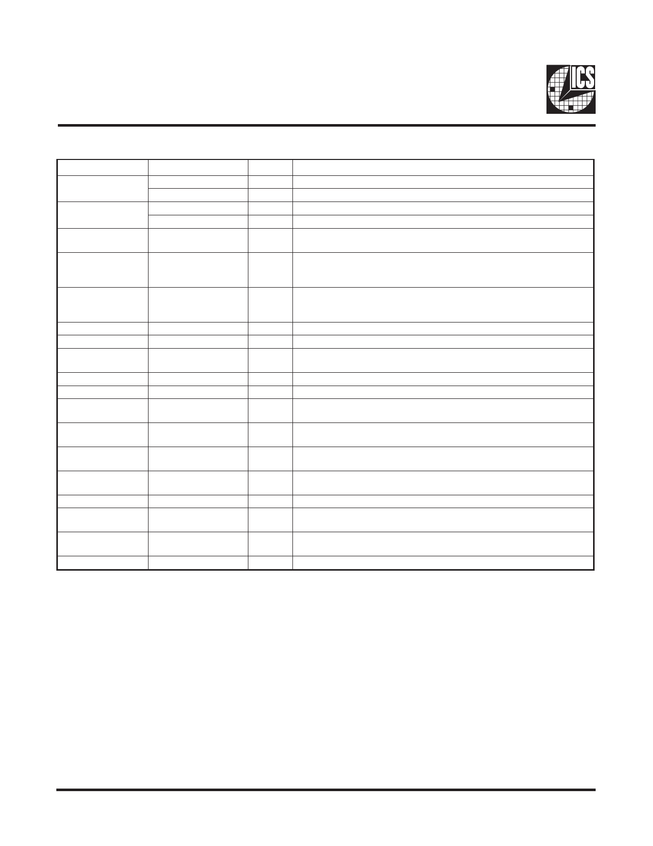
Pin Descriptions
PIN NUM BER
1
2
3, 10, 17, 24, 31,
37, 43
PIN NAM E
REF2
FS2
REF1
FS1
GND
4
X1
5
X2
7, 15, 28, 34 VDD3
8,9,11,12,13,14,16 BUSF, BUS(1:6)
18
FSO
21, 25, 48
22, 23
VDD
48, 24MHz
26
BUSSTOP#
27
CPUSTOP#
36, 35, 33, 32, 30,
29
SDRAM (1:6)
40, 46
VDD2
41, 42, 39,38 CPU (1:4)
44
PD#
45
6, 19, 20, 47
IOAPIC
N/C
TYPE
OUT
IN
OUT
IN
D ES CR IPTION
Reference clock output*
Logic input frequency select Bit 2*
Reference clock output*
Logic input frequency select Bit1*
PWR Ground.
IN
OUT
PWR
OUT
IN
PWR
OUT
IN
IN
OUT
PWR
OUT
IN
OUT
—
Crystal input. Nominally 14.318 MHz. Has internal load cap. External
crystal load of 30pF to GND recommended for VDD power on faster
than 2.0ms.
Crystal output. Has internal load cap and feedback resistor to X1.
External crystal load of 10pF to GND recommended for VDD power
on faster than 2.0ms.
3.3V I/O power supply, BUS and SDRAM buffer supply.
BUS clock outputs. see select table for frequency
Select pin for enabling 66.6 MHz or 60 MHz, or other selections in
frequency select table.
Core power supply, and fixed clock power.
48, 24MHz clock outputs
Input pin to synchronously stop all BUS (1:6) clocks when pin is
low.
Input pin to synchronously stop all CPU and SDRAM clocks when
pin is low.
SDRAM clocks at CPU speed. See select table for frequency.
Powered by VDD3.
2.5V Power Supply for CPU and IOAPIC buffers, can be tied to
VDD3 for 3.3V operation
CPU clock output clocks .See select table for frequency
Power down logic control input. When low, powers off both PLL
and all outputs forced to logic low.
IOAPIC clock output (Freq=14.318 with nominal crystal) Powered
by VDD2 supply
Pins not internally connected.
* Bidirectional input/output pins, input logic levels are latched at internal power-on-reset. Use 10Kohm resistor to program logic
Hi to VDD or GND for logic low.
2
Share Link: 