HC4052 데이터 시트보기 (PDF) - Philips Electronics
부품명
상세내역
일치하는 목록
HC4052 Datasheet PDF : 27 Pages
| |||
Philips Semiconductors
Dual 4-channel analog multiplexer,
demultiplexer
Product specification
74HC4052; 74HCT4052
FEATURES
• Wide analog input voltage range from −5 V to +5 V
• Low ON-resistance:
– 80 Ω (typical) at VCC − VEE = 4.5 V
– 70 Ω (typical) at VCC − VEE = 6.0 V
– 60 Ω (typical) at VCC − VEE = 9.0 V
• Logic level translation: to enable 5 V logic to
communicate with ±5 V analog signals
• Typical “break before make” built in
• Complies with JEDEC standard no. 7A
• ESD protection:
– HBM EIA/JESD22-A114-B exceeds 2000 V
– MM EIA/JESD22-A115-A exceeds 200 V.
• Specified from −40 °C to +85 °C and −40 °C to +125 °C.
APPLICATIONS
• Analog multiplexing and demultiplexing
• Digital multiplexing and demultiplexing
• Signal gating.
DESCRIPTION
The 74HC4052 and 74HCT4052 are high-speed Si-gate
CMOS devices and are pin compatible with the
HEF4052B. They are specified in compliance with JEDEC
standard no. 7A.
The 74HC4052 and 74HCT4052 are dual 4-channel
analog multiplexers or demultiplexers with common select
logic. Each multiplexer has four independent
inputs/outputs (pins nY0 to nY3) and a common
input/output (pin nZ). The common channel select logics
include two digital select inputs (pins S0 and S1) and an
active LOW enable input (pin E). When pin E = LOW, one
of the four switches is selected (low-impedance ON-state)
with pins S0 and S1. When pin E = HIGH, all switches are
in the high-impedance OFF-state, independent of pins S0
and S1.
VCC and GND are the supply voltage pins for the digital
control inputs (pins S0, S1, and E). The VCC to GND
ranges are 2.0 V to 10.0 V for 74HC4052 and
4.5 V to 5.5 V for 74HCT4052. The analog inputs/outputs
(pins nY0 to nY3 and nZ) can swing between VCC as a
positive limit and VEE as a negative limit. VCC − VEE may
not exceed 10.0 V.
For operation as a digital multiplexer/demultiplexer, VEE is
connected to GND (typically ground).
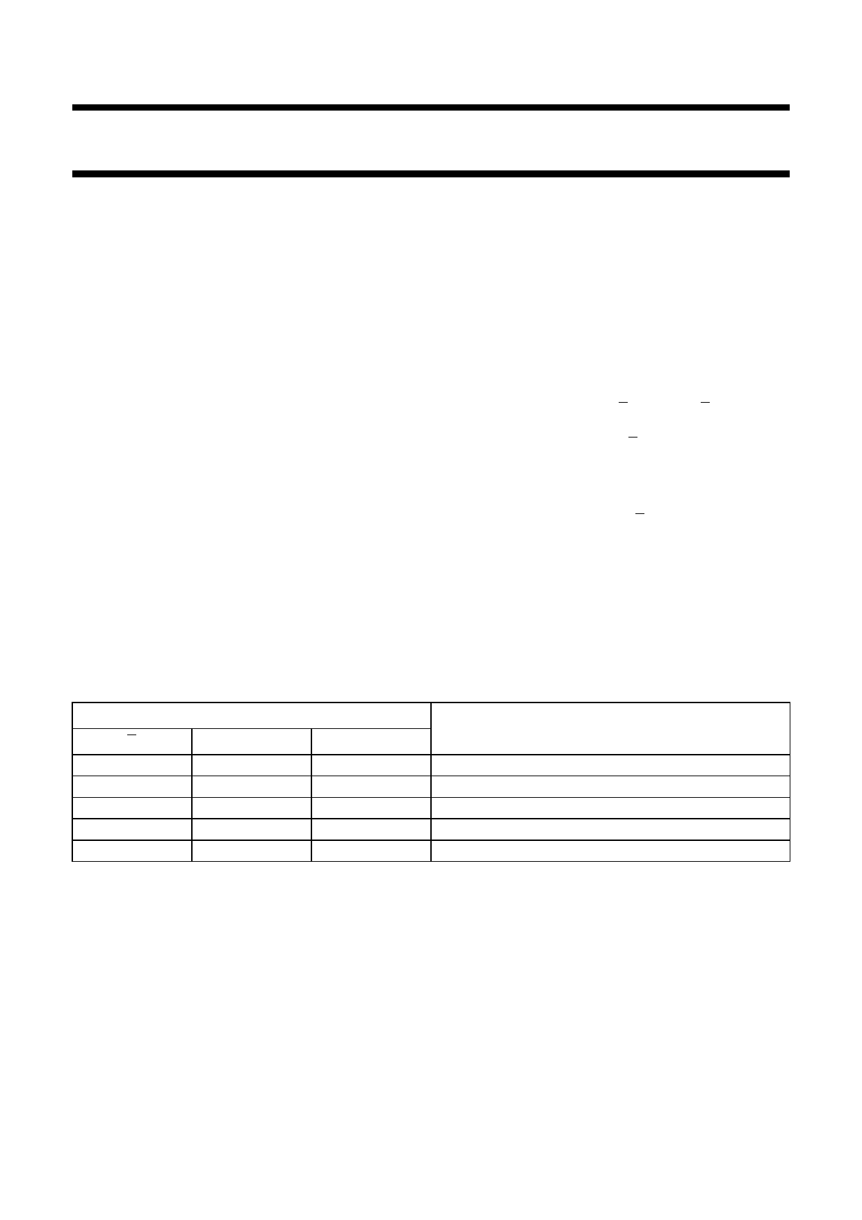
FUNCTION TABLE
INPUT(1)
E
S1
L
L
L
L
L
H
L
H
H
X
Note
1. H = HIGH voltage level
L = LOW voltage level
X = don’t care.
CHANNEL BETWEEN
S0
L
nY0 and nZ
H
nY1 and nZ
L
nY2 and nZ
H
nY3 and nZ
X
none
2004 Nov 11
2
Share Link: 