G914 데이터 시트보기 (PDF) - Global Mixed-mode Technology Inc
부품명
상세내역
일치하는 목록
G914 Datasheet PDF : 6 Pages
| |||
Global Mixed-mode Technology Inc.
G914
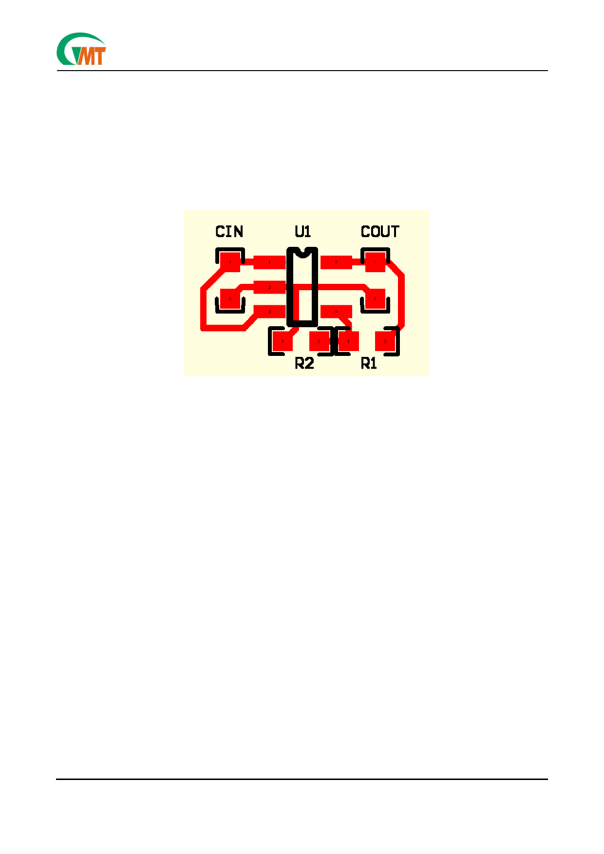
Layout Guide
An input capacitance of ≅ 1µF is required between the
G914 input pin and ground (the amount of the capaci-
tance may be increased without limit), This capacitor
must be located a distance of not more than 1cm from
the input and return to a clean analog ground.
Input capacitor can filter out the input voltage spike
caused by the surge current due to the inductive effect
of the package pin and the printed circuit board’s
routing wire. Otherwise, the actual voltage at the IN
pin may exceed the absolute maximum rating.
The output capacitor also must be located a distance
of not more than 1cm from output to a clean analog
ground. Because it can filter out the output spike
caused by the surge current due to the inductive effect
of the package pin and the printed circuit board’s
routing wire. Figure 3 is suggested PCB layout of
G914.
Figure 3. Suggested PCB Layout
*Distance between pin & capacitor must no more than 1cm
Ver 0.1 Preliminary
Nov 05, 2001
TEL: 886-3-5788833
http://www.gmt.com.tw
5
Share Link: 