G914 데이터 시트보기 (PDF) - Global Mixed-mode Technology Inc
부품명
상세내역
일치하는 목록
G914 Datasheet PDF : 6 Pages
| |||
Global Mixed-mode Technology Inc.
G914
Absolute Maximum Ratings
VIN to GND……………………………………-0.3V to +7V
Output Short-Circuit Duration………………….….Infinite
SET to GND.……………………………..…..-0.3V to +7V
SHDN to GND…………………..………….-0.3V to +7V
SHDN to IN….…………………..…………..-7V to +0.3V
OUT to GND…………………………-0.3V to (VIN + 0.3V)
Continuous Power Dissipation (TA = +25°C)
SOT23-5……………………………………...…..568 mW
Operating Temperature Range………...-40°C to +85°C
Junction Temperature……………………….……+150°C
θJA….…..……………….…………….…..…..220°C/Watt
Storage Temperature Range………….-65°C to +160°C
Lead Temperature (soldering, 10sec)..…………+300°C
Stresses beyond those listed under "Absolute Maximum Ratings" may cause permanent damage to the device. These are stress rat-
ings only, and functional operation of the device at these or any other conditions beyond those indicated in the operational sections of
the specifications is not implied. Exposure to absolute maximum rating conditions for extended periods may affect device reliability.
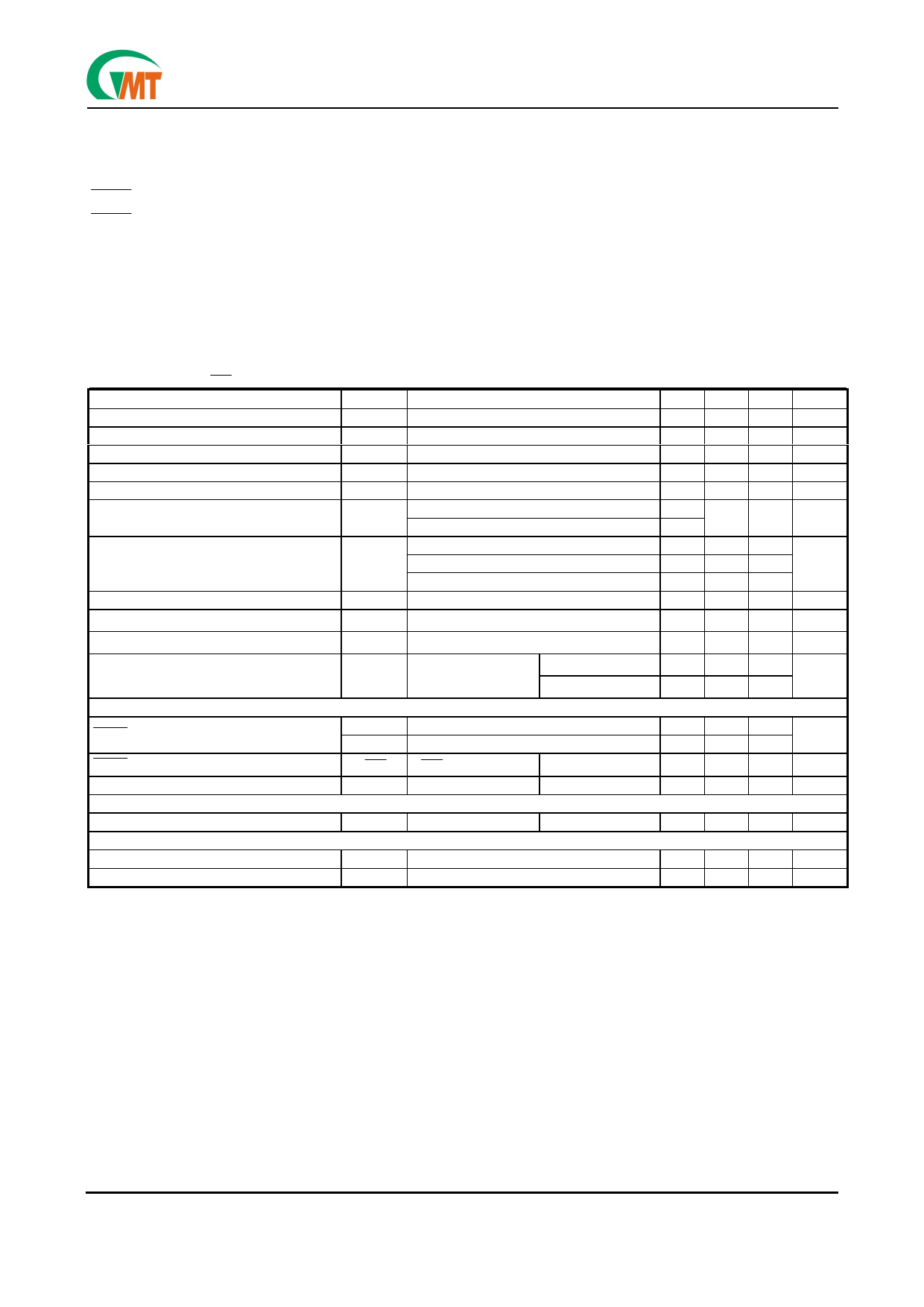
Electrical Characteristics
(VIN = VOUT +1V; VSHDN = VIN; CIN = COUT = 1µF = TA = TJ = +25°C, unless otherwise noted.) (Note 1)
PARAMETER
SYMBOL CONDITIONS
MIN TYP MAX UNITS
Input Voltage (Note 2)
Output Voltage Accuracy
Adjustable Output Voltage Range (Note 3)
Maximum Output Current
VIN
VOUT
VOUT
Variation from specified VOUT, IOUT=1mA
Note2
-2
2.5
150
5.5
V
2
%
5.5
V
mA
Current Limit
Ground Pin Current
Dropout Voltage (Note 3)
Line Regulation
ILIM
IQ
VDROP
∆VLNR
VOUT = 0V
ILOAD = 0mA
ILOAD = 150mA
IOUT = 1mA
IOUT = 50mA
IOUT =150mA
VIN=VO +0.1V to 5.5V, IOUT = 1mA
370
mA
52 80
µA
2
100
mV
340
0.1
%/V
Load Regulation
∆VLDR IOUT = 0mA to 150mA
30
mV
Output Voltage Temperature Coefficient ∆VO / ∆T IOUT = 40mA, TJ = 25°C to 125°C
40
ppm/°C
Output Voltage Noise (10HZ to 100KHZ)
en IL = 150mA
CADJ = 470pF
CADJ = 10nF
192
µVRMS
170
SHUTDOWN
SHDN Input Threshold
SHDN Input Bias Current
VIH
VIL
I SHDN
Regulator enabled
Regulator shutdown
V SHDN = VIN
TA = +25°C
2
V
0.4
0.007 0.1 µA
Shutdown Supply Current
ADJ INPUT
IQSHDN VOUT = 0V
TA = +25°C
0.06 1
µA
ADJ Input Leakage Current
THERMAL PROTECTION
IADJ VADJ = 1.3V
TA = +25°C
5
20
nA
Thermal Shutdown Temperature
Thermal Shutdown Hysteresis
TSHDN
∆TSHDN
150
°C
15
°C
Note 1: Limits is 100% production tested at TA= +25°C. Low duty pulse techniques are used during test to
maintain junction temperature as close to ambient as possible.
Note 2: VIN (min) = VOUT +VDROP.
Note 3: The dropout voltage is defined as (VIN-VOUT) when VOUT is 100mV below the value of VOUT for VIN = VOUT +2V.
Ver 0.1 Preliminary
Nov 05, 2001
TEL: 886-3-5788833
http://www.gmt.com.tw
2
Share Link: 