TDA8948J/N1112 데이터 시트보기 (PDF) - NXP Semiconductors.
부품명
상세내역
일치하는 목록
TDA8948J/N1112 Datasheet PDF : 26 Pages
| |||
NXP Semiconductors
TDA8948J
4-channel audio amplifier
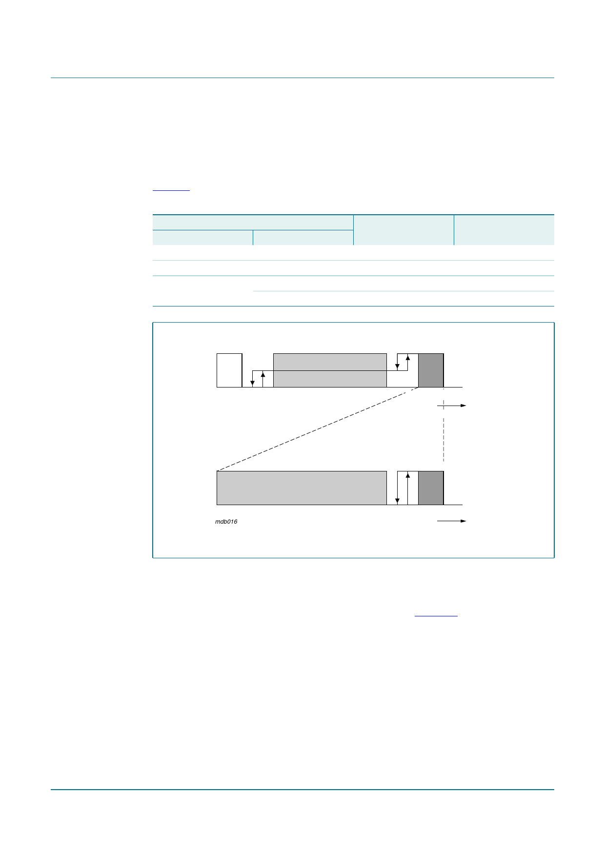
On - The amplifier is operating normally. The on mode is activated at
VMODE1 > (VCC − 2.0 V). The output of channels 3 and 4 can be set to mute or on mode.
The output channels 3 and 4 can be switched on/off by applying a proper DC voltage to
pin MODE2, under the condition that the output channels 1 and 2 are in the on mode (see
Figure 3).
Table 5. Mode selection
Voltage on pin
MODE1
MODE2
0 V to 0.8 V
4.5 V to (VCC − 3.5 V)
(VCC − 2.0 V) to VCC
0 V to VCC
0 V to VCC
0 V to (VCC − 3.5 V)
(VCC − 2 V) to VCC
Channel 1 and 2
Standby mode
Mute mode
On mode
On mode
Channel 3 and 4
(sub woofer)
Standby mode
Mute mode
Mute mode
On mode
all standby
all mute
channels 1 + 2: on
channels 3 + 4: on or mute
0.8
4.5
VCC−3.5 VCC−2.0 VCC
VMODE1
channels 3 + 4: mute
channels 3 + 4: on
mdb016
Fig 3. Mode selection
VCC−3.5 VCC−2.0 VCC
VMODE2
8.4 Supply voltage ripple rejection
The Supply Voltage Ripple Rejection (SVRR) is measured with an electrolytic capacitor of
150 µF on pin SVR using a bandwidth of 20 Hz to 22 kHz. Figure 10 illustrates the SVRR
as function of the frequency. A larger capacitor value on pin SVR improves the ripple
rejection behavior at the lower frequencies.
TDA8948J_1
Product data sheet
Rev. 01 — 27 February 2008
© NXP B.V. 2008. All rights reserved.
7 of 26
Share Link: 