TDA8948J/N1112 데이터 시트보기 (PDF) - NXP Semiconductors.
부품명
상세내역
일치하는 목록
TDA8948J/N1112 Datasheet PDF : 26 Pages
| |||
NXP Semiconductors
TDA8948J
4-channel audio amplifier
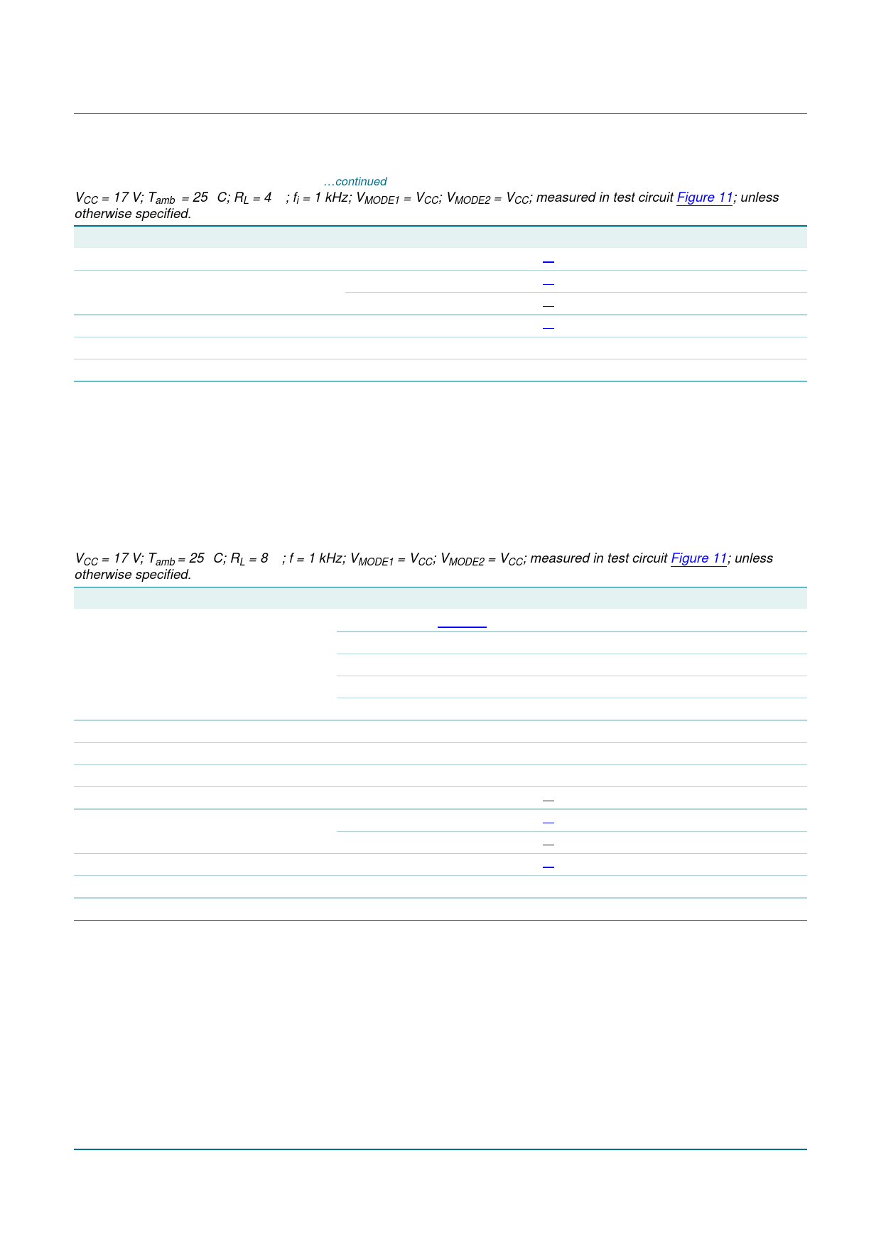
Table 9. Dynamic characteristics SE …continued
VCC = 17 V; Tamb = 25 °C; RL = 4 Ω; fi = 1 kHz; VMODE1 = VCC; VMODE2 = VCC; measured in test circuit Figure 11; unless
otherwise specified.
Symbol Parameter
Conditions
Min
Typ
Max
Unit
Vn(o)
SVRR
Vo(mute)
αcs
|∆Gv|
output noise voltage
supply voltage ripple rejection
mute output voltage
channel separation
voltage gain difference
-
fripple = 1 kHz
fripple = 100 Hz to 20 kHz
-
RSOURCE = 0 Ω
-
[1] -
[2] -
[2] -
[3] -
50
-
150
-
µV
60
-
dB
60
-
dB
-
150
µV
60
-
dB
-
1
dB
[1] The noise output voltage is measured at the output in a frequency range from 20 Hz to 22 kHz (unweighted), with a source impedance
RSOURCE = 0 Ω at the input.
[2] Supply voltage ripple rejection is measured at the output, with a source impedance RSOURCE = 0 Ω at the input and with a frequency
range from 20 Hz to 22 kHz (unweighted). The ripple voltage is a sine wave with a frequency fripple and an amplitude of 300 mV (RMS),
which is applied to the positive supply rail.
[3] Output voltage in mute mode is measured with VMODE1 = VMODE2 = 7 V, and Vi = 1 V (RMS) in a bandwidth from 20 Hz to 22 kHz,
including noise.
Table 10. Dynamic characteristics BTL
VCC = 17 V; Tamb = 25 °C; RL = 8 Ω; f = 1 kHz; VMODE1 = VCC; VMODE2 = VCC; measured in test circuit Figure 11; unless
otherwise specified.
Symbol Parameter
Conditions
Min
Typ
Max
Unit
Po(BTL)
THD
Gv
Zi
Vn(o)
SVRR
Vo(mute)
αcs
|∆Gv|
BTL output power
total harmonic distortion
voltage gain
input impedance
noise output voltage
supply voltage ripple rejection
mute output voltage
channel separation
voltage gain difference
VCC = 17 V; see Figure 7
THD = 10 %; RL = 8 Ω
THD = 0.5 %; RL = 8 Ω
VCC = 20 V
THD = 10 %; RL = 8 Ω
Po = 1 W
-
-
-
fripple = 1 kHz
fripple = 100 Hz to 20 kHz
-
RSOURCE = 0 Ω
-
14
-
-
-
31
20
[1] -
[2] -
[2] -
[3] -
50
-
16
-
W
12
-
W
24
-
W
0.05
0.5
%
32
33
dB
30
-
kΩ
200
-
µV
65
-
dB
65
-
dB
-
250
µV
65
-
dB
-
1
dB
[1] The noise output voltage is measured at the output in a frequency range from 20 Hz to 22 kHz (unweighted), with a source impedance
RSOURCE = 0 Ω at the input.
[2] Supply voltage ripple rejection is measured at the output, with a source impedance RSOURCE = 0 Ω at the input and with a frequency
range from 20 Hz to 22 kHz (unweighted). The ripple voltage is a sine wave with a frequency fripple and an amplitude of 300 mV (RMS),
which is applied to the positive supply rail.
[3] Output voltage in mute mode is measured with VMODE1 = VMODE2 = 7 V, and Vi = 1 V (RMS) in a bandwidth from 20 Hz to 22 kHz,
including noise.
TDA8948J_1
Product data sheet
Rev. 01 — 27 February 2008
© NXP B.V. 2008. All rights reserved.
10 of 26
Share Link: 