MP3213 데이터 시트보기 (PDF) - Monolithic Power Systems
부품명
상세내역
일치하는 목록
MP3213 Datasheet PDF : 10 Pages
| |||
MP3213 – 700KHZ/1.3MHZ BOOST CONVERTER WITH A 3.5A SWITCH
Compensation
The output of the transconductance error
amplifier (COMP) is used to compensate the
regulation control system. The system uses two
poles and one zero to stabilize the control loop.
The poles are fP1 set by the output capacitor C2
and load resistance and fP2 set by the
compensation capacitor C3. The zero fZ1 is set
by the compensation capacitor C3 and the
compensation resistor R3. These are
determined by the equations:
fP1
=
1
π × C2 × RLOAD
fP2
=
GEA
2 × π × C3 × A VEA
f Z1
=
2×
1
π × C3 × R3
Where RLOAD is the load resistance, GEA is the
error amplifier transconductance, and AVEA is
the error amplifier voltage gain.
The DC loop gain is:
A VDC
= 1.5 × A VEA
× VIN × R LOAD
VOUT 2
× VFB
Where VFB is the feedback regulation threshold.
There is also a right-half-plane zero (fRHPZ) that
exists in continuous conduction mode (inductor
current does not drop to zero on each cycle)
step-up converters. The frequency of the right
half plane zero is:
fRHPZ
=
VIN2 × RLOAD
2× π ×L × VOUT 2
Table 1 lists generally recommended
compensation components for different input
voltage, output voltage and capacitance of most
frequently used output ceramic capacitors.
Ceramic capacitors have extremely low ESR,
therefore the second compensation capacitor
(from COMP to GND) is not required.
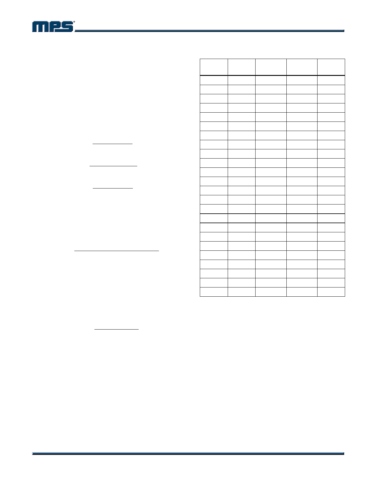
Table 1—Component Selection
VIN
VOUT
C2
(V)
(V)
(µF)
3.3
8
4.7
3.3
8
10
3.3
8
22
3.3
12
4.7
3.3
12
10
3.3
12
22
3.3
18
4.7
3.3
18
10
3.3
18
22
5
8
4.7
5
8
10
5
8
22
5
12
4.7
5
12
10
5
12
22
5
18
4.7
5
18
10
5
18
22
12
15
4.7
12
15
10
12
15
22
12
18
4.7
12
18
10
12
18
22
R3
C3
(kΩ)
(nF)
10
2.2
10
2.2
10
2.2
15
1
15
1
15
2.2
20
1
20
1
30
2.2
10
4.7
10
4.7
15
1
15
2.2
15
2.2
20
1
20
1
20
1
30
1
10
2.2
10
2.2
15
1
5.1
2.2
5.1
2.2
15
1
For faster control loop and better transient
response, set the capacitor C3 to the
recommended value in Table 1. Then slowly
increase the resistor R3 and check the load
step response on a bench to make sure the
ringing and overshoot on the output voltage at
the edge of the load steps is minimal. Finally,
the compensation needs to be checked by
calculating the DC loop gain and the crossover
frequency. The crossover frequency where the
loop gain drops to 0dB or a gain of 1 can be
obtained visually by placing a –20dB/decade
slope at each pole, and a +20dB/decade slope
at each zero. The crossover frequency should
be at least one decade below the frequency of
the right-half-plane zero at maximum output
load current to obtain high enough phase
margin for stability.
MP3213 Rev. 1.1
www.MonolithicPower.com
8
5/12/2006
MPS Proprietary Information. Unauthorized Photocopy and Duplication Prohibited.
© 2006 MPS. All Rights Reserved.
Share Link: 