CH1786NH 데이터 시트보기 (PDF) - Cermetek Microelectronics
부품명
상세내역
일치하는 목록
CH1786NH Datasheet PDF : 18 Pages
| |||
Cermetek Microelectronics, Inc.
CH1786 Family of Ultra Small 2400bps Modems
upon an input low signal on the TXD pin.
ATS24=255 disables the Sleep Mode and is the
default if no value is set in register S24.
A SLEEP output signal is available to control power to
external devices. In Figure 6, a FET controlled by the
SLEEP signal turns of the external speaker amplifier
when the CH1786 enters Sleep Mode. In Sleep
Mode, power is reduced to approximately 50% of
normal operating power.
Guard Tone. A guard tone of 550 Hz or 1800 Hz can
be generated at 6 dB or 9 dB below the transmit level,
respectively, by using the &Gn command. Refer to
“Cermetek AT Commands and S-Registers reference
Guide” or the Cermetek web site at
http://www.cermetek.com.
pin becomes active. The CH1786ET products can
thus be powered down to zero.
Table 1. Connection Rates.
Answering
Connection Rate Resulting
Modem Initial
When Calling Modem Initial
Trained Rate
Rate Is:
300
1200
2400
300
300
1200
1200
1200
300
1200
1200
2400
300
1200
2400
Answer Tone. A CCITT (2100 Hz) or Bell (2225Hz)
answer tone is generated depending on the selected
configuration. Refer to “Cermetek AT commands and
S-Registers Reference Guide” or the Cermetek web
site at http://www.cermetek.com.
Data Encoding. The data encoding conforms to
CCITT recommendations V.22bis or V.22, or
Bell212A, or 103, depending on the selected
configuration. Refer to “Cermetek AT commands and
S-Register Reference Guide” or the Cermetek web
site at http://www.cermetek.com.
Line Equalization. Transmitter and receiver digital
filters compensate for delay and amplitude distortion
during operation on nominal phone lines. In addition,
automatic adaptive equalization in the receiver
minimizes the effects of inter symbol interference.
Transmission Speed. In normal operation, the
originating modem initiates the call and attempts to
connect to the answering modem at a speed
established by the originating modem’s controller
prior to call initiation. This is referred to as the Initial
Trained Rate. Upon receiving the call, the answering
modem will attempt to connect to the originating
modem at its Initial Trained Rate. If these two rates
are identical, the connection is made. If the speeds
differ, the answering modem must adjust its rate or
terminate the call. Table 1 indicates the connection
rate that will result when the calling modem’s Initial
Trained Rate and the answering modem’s Initial
Trained Rate are different.
NOTE
A 2400-baud connection rate will only result if both
modems are initially set at 2400 baud.
Zero Power Mode (CH1786ET only). If an
application calls for zero power during standby
periods, the power may be switched off using external
circuitry and then reapplied when the CH1786 ’s RI
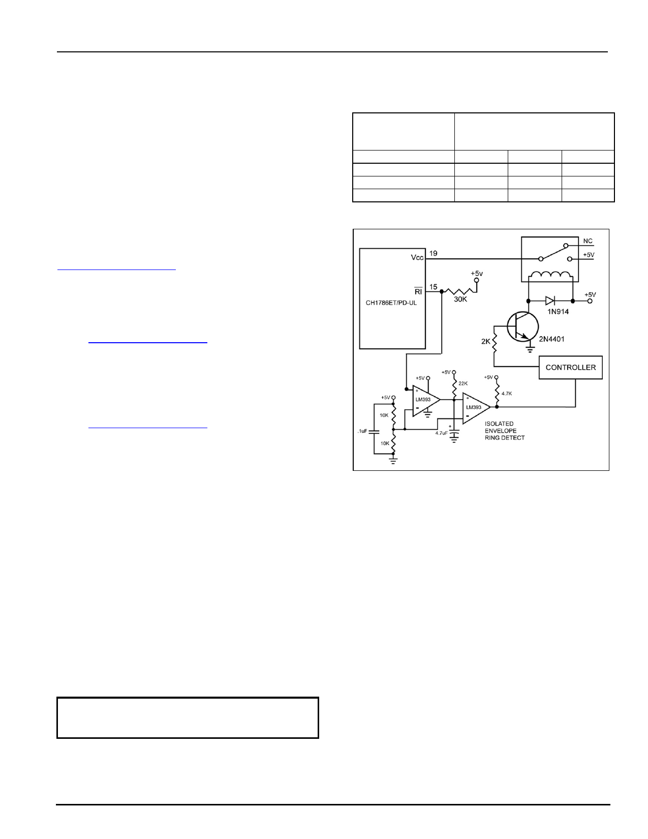
Figure 3. Zero Power Operation.
Referring to Figure 3, the controller activates the relay
switch, supplying power (+5V) to the CH1786ET. In
this configuration, the ring signal is used to “wake up”
the CH1786ET when the CH1786ET is in the power
down state.
The pins of the CH1786ET will be in an undefined
state when power is switched off. This must be taken
into consideration to assure that no unwanted signals
are presented to the CH1786ET during power down.
Ring Indicator (RI). The RI pin follows the frequency
of the ring signal and toggles low when the CH1786
detects an incoming call. The ring signal is typically
20 to 30 Hz and is on for 2 seconds and off for 4
seconds. Although not TTL compliant, the RI pin can,
nonetheless, be utilized to activate external circuitry
including the external RST pin.
When using the RI pin, it is recommended that a
Schmitt Trigger or the Isolated Envelope Detect
Circuit in Figures 3 or 5 be placed between the RI pin
and the external load.
Power Supply. The CH1786 modem module is a
complex set of sub-systems. During the course of
2003 Cermetek Microelectronics, Inc.
Page 3
Document No. 607-0004 Revision L1 (06/03)
Share Link: 