T7264 데이터 시트보기 (PDF) - Agere -> LSI Corporation
부품명
상세내역
일치하는 목록
T7264 Datasheet PDF : 54 Pages
| |||
T7264 U-Interface 2B1Q Transceiver
Data Sheet
April 1998
Pin Information (continued)
Table 3. Clock Configuration
VDDO
+5 V
+5 V
+5 V
+5 V
0V
0V
MCLK
0
0
1
1
15.36 MHz
15.36 MHz
CKSEL
0
1
0
1
0
1
CKOUT*
15.36 MHz (free-running)
10.24 MHz (phase-locked)
7.68 MHz (free-running)
3-stated (default)
15.36 MHz (free-running)
3-stated
* The 10.24 MHz CKOUT is high for one-half of a 15.36 MHz period and low for one 15.36 MHz period. To compensate for the difference be-
tween the phase-locked and free-run frequencies, one-half 15.36 MHz clock periods are occasionally either removed from or added to the low
time of the 10.24 MHz period.
Functional Overview
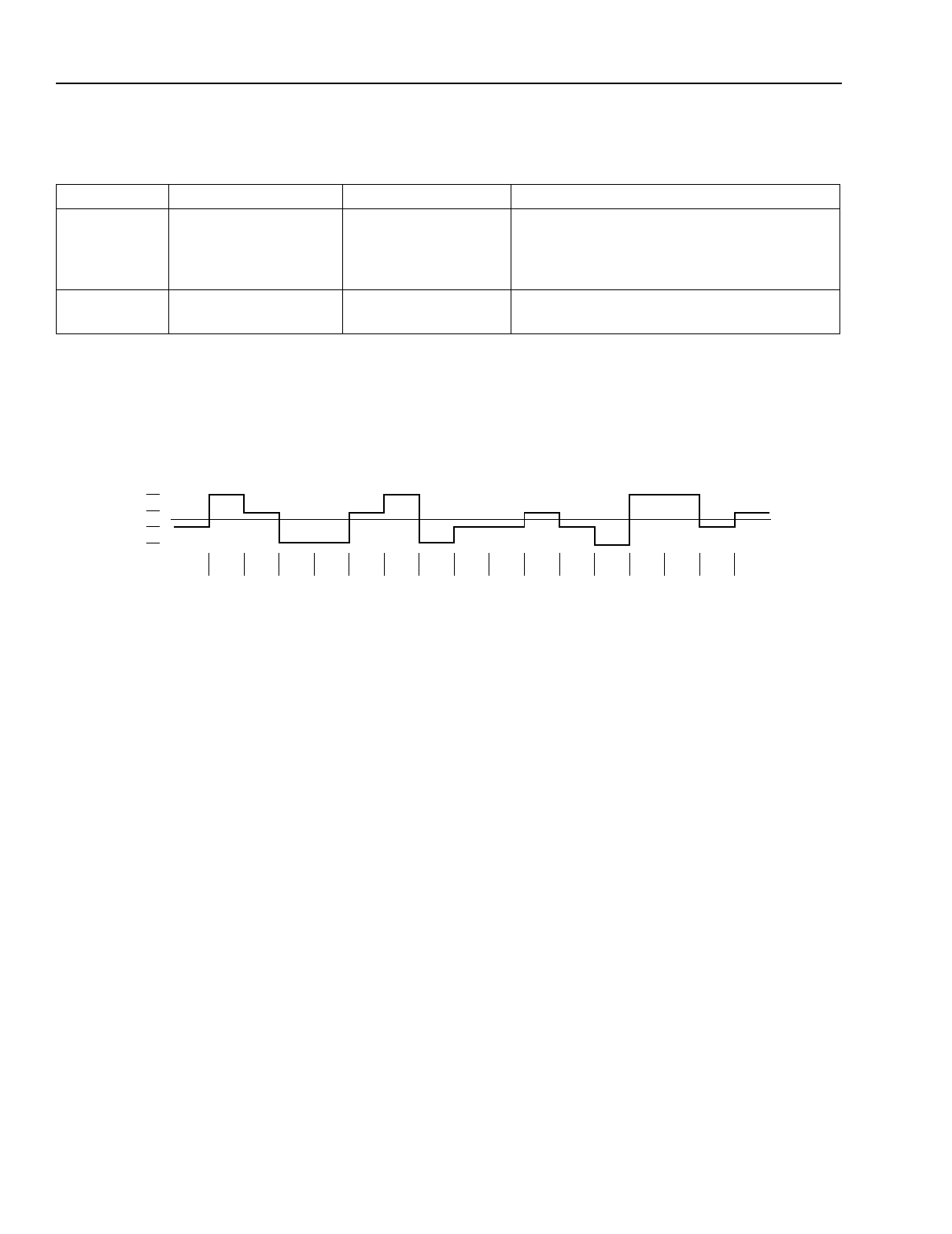
+3
+1
–1
–3
QUAT –1 +3 +1 –3 –3 +1 +3 –3 –1 –1 +1 –1 –3 +3 +3 –1 +1
BITS 01 10 11 00 00 11 10 00 01 01 11 01 00 10 10 01 11
Figure 3. Quat Example
5-5162F
The T7264 chip conforms to the T1.601 ANSI North
American 1992 Standard for 2B1Q line encoding. The
2B1Q line code provides a four-level pulse amplitude
modulation code with no redundancy. Data is grouped
into pairs of bits for conversion to quaternary (quat)
symbols. Figure 3 above shows an example of this cod-
ing method.
The analog front end provides the 2B1Q line coder
(D/A conversion), pulse shaper, line driver, first-order
line balance network, crystal oscillator clock genera-
tion, and sigma-delta A/D conversion. The line driver
provides pulses which allow the 2.5 V template of the
T1.601 specification to be met when connected to the
proper transformer and interface circuitry. The A/D con-
verter is implemented using a double-loop, sigma-delta
modulator.
A crystal oscillator provides the 15.36 MHz master
clock for the chip. An on-chip, digital phase-locked loop
provides the ability to synchronize the chip clock to the
system clock in the LT or to the line clock in the NT.
Provisions are made for using either an on-chip crystal
oscillator with an external crystal, or using an external
clock source.
The T7264 takes input at the K2 interface and formats
this information for the U-interface through a scram-
bling algorithm and the addition of synchronization bits
for U framing. This data is then transferred to the 2B1Q
encoder for transmission over the U loop. Signals com-
ing from the U loop are first passed through the sigma-
delta A/D converter and then sent for extensive signal
processing. The T7264 provides decimation of the
sigma-delta output (DEC), linear and nonlinear echo
cancellation, automatic gain control (AGC), signal
detection, decision feedback equalization (DFE), timing
recovery (TR), descrambling, line-code polarity detec-
tion, and rate adaption for output onto the K2 interface.
The DFE circuit provides the functionality necessary for
proper operation on subscriber loops with bridged taps.
6
Lucent Technologies Inc.
Share Link: 