T7264 데이터 시트보기 (PDF) - Agere -> LSI Corporation
부품명
상세내역
일치하는 목록
T7264 Datasheet PDF : 54 Pages
| |||
T7264 U-Interface 2B1Q Transceiver
Data Sheet
April 1998
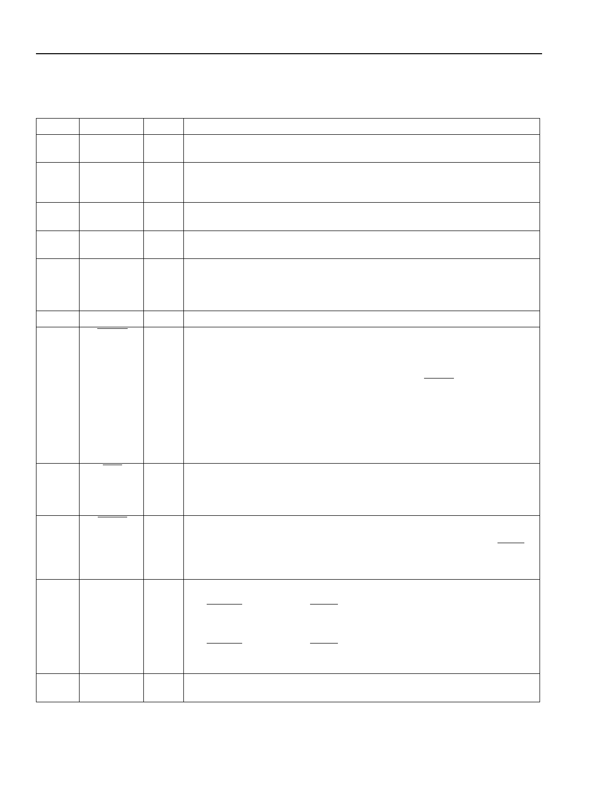
Pin Information (continued)
Table 2. Pin Descriptions
Pin
1
2
3
4
5
6, 17
7
8
9
10, 11
12, 22,
27, 44
Symbol
DI
MTC
C
DO
F
VDDD
RESET
FFC
ILOSS
MODE[0:1]
GNDD
Type
I
I
O
O
O
P
I
I
I
I
P
Name/Function
K2 Transmit Data Input. Serial data input passing transmit data across K2 in-
terface at 512 kbits/s. Latched on falling edge of C clock.
Master Timing Clock. 8 kHz clock input. In LT mode (MODE0 = 1), all clocks
except CKOUT in the 15.36 MHz and 7.68 MHz modes are locked to this input
clock. In the NT mode (MODE0 = 0), this input is not used.
512 kbits/s K2 Bit Clock Output. Synchronized to F. Defines K2 bit period (ris-
ing edge to rising edge).
K2 Receive Data Output. Serial data output passing receive data across K2 in-
terface at 512 kbits/s. Changes on the rising edge of C clock.
8 kHz Clock Output. Defines K2 frame (rising edge to rising edge). In LT mode
(MODE0 = 1), this clock is locked to MTC at 0° phase shift with ±65 ns of jitter
(for jitter-free MTC). In NT mode (MODE0 = 0), this clock is derived from the
U-interface signal.
+5 V Supply for Digital Circuits. Internally connected together.
Reset (Active-Low). Asynchronous Schmitt trigger input. This pin maintains
the transceiver in reset indefinitely without the need to access the K2 interface.
It must be held low for three consecutive F clock periods for active or idle mode
or 1.5 ms after power on. After power-on reset or idle mode reset, an additional
1.0 ms is required before the device is fully functional. RESET overrides all other
transceiver control signals, halts loop transmission, clears the transceiver adap-
tive filter coefficients, and resets the phase-locked loop. After a reset, the next
activation is a cold start. Unlike afrst (software reset via the K2 interface), when
this pin is held low, synchronization is lost between F and MTC (LT). After this
pin goes high, F and MTC regain synchronization. All output clocks remain func-
tional during reset.
Freeze Frequency Control (Active-Low). Asynchronous input. Freeze the
clock frequency control (i.e., the internal state variables of the timing recovery
remain constant). This control is operative in both LT and NT modes. This pin is
latched on the rising edge of every RCLKEN.
Insertion Loss Test (Active-Low). NT ONLY. When enabled, the transmitter
continuously transmits the sequence SN1. The receiver remains reset. The
transceiver performs a reset when this pin returns to its inactive state. ILOSS is
latched on the rising edge of F. Leave this pin unconnected or tied to VDD in LT
mode.
Mode 0 and 1. Two-pin field selecting chip mode:
MODE0
Action
0
Configure for chip being used on the NT end of loop.
1
Configure for chip being used on the LT end of loop.
MODE1
Action
0
Disables autoreporting of nebe to febe.
1
Enables autoreporting of nebe to febe.
Ground Supply for Digital Circuits. Internally connected together.
4
Lucent Technologies Inc.
Share Link: 