NJU6624CFG1 데이터 시트보기 (PDF) - Japan Radio Corporation
부품명
상세내역
일치하는 목록
NJU6624CFG1
Japan Radio Corporation

NJU6624CFG1 Datasheet PDF : 27 Pages
| |||
NJU6624C
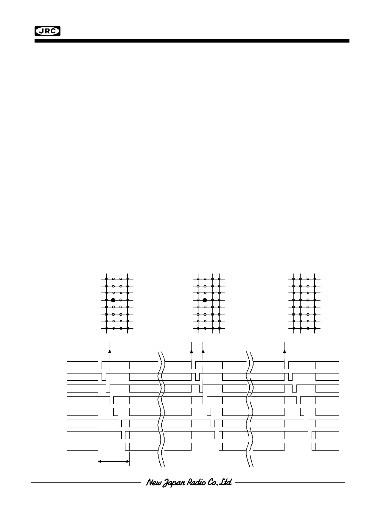
(1-9)Keyscan circuit
The Keyscan circuit consists of a detector block of key pressing and a fetching block of key status. It scans 4x8
key matrix and fetches conditions of 32 keys. Furthermore, it operates correctly against the key roll over input.
-Request signal output
When the NJU6624C detect the key pressing by the key scan circuit, it outputs “H” signal as the request signal
from the “REQ” terminal to notice the key pressing information to an application system.
-Contents of key register renewal
Contents of key register are “0000 0000” in case of no key operation. Contents of key register are not changed in
busy of key data reading operation. Key data is fetched into the key register after 2 clock of the end of a keyscan
cycle and kept by the start of next cycle.
-Key data input terminal and segment terminal
Keyscan signal output terminals operate as segment terminals (SEG1 to SEG8) also and keyscan signals are
output in interval period of segment signals. Key data input terminals (K0 to K3) are pulled up to VDD in busy of
keyscan operation (tKS). In this period, terminals of SEG9 to SEG70 output the voltage of V2 or VLCD2.
-Keyscan OFF mode
Keyscan operation is turned ON or OFF by the instruction. In case of keyscan OFF, the detector of key pressing
is not operating and key data input terminals (K0 to K3) are not pulled up during the period of keyscan (tKS). In
the period of keyscan (tKS), all of segment terminals (SEG1 to SEG70) output the voltage of V2 or VLCD2.
-Example Keyscan
S0
S0
S0
S1
S1
S1
S2
S2
S2
S3
S3
S3
S4
S4
S4
S5
S5
S5
S6
S6
S6
S7
S7
S7
REQ
SEG1/S0
SEG2/S1
SEG3/S2
SEG4/S3
SEG5/S4
SEG6/S5
SEG7/S6
SEG8/S7
tKS
Share Link: