TEA5170 데이터 시트보기 (PDF) - STMicroelectronics
부품명
상세내역
일치하는 목록
TEA5170 Datasheet PDF : 9 Pages
| |||
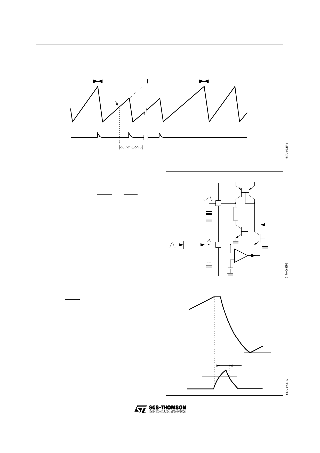
Figure 3
UNSYNCHRONIZED
MODE
Vct
Vtsy
SYNCHRONIZED MODE
TEA5170
UNSYNCHRONIZED
MODE
Vrt
Wtrig- Wtrig+
Remark : In case of an application between
TEA5170 and TEA2164, to optimize the
synchronization windows of these
circuits, the following relations have to
be
used
:
Tm
=
T1S.Y0N6CTe
=
Tm
1.223
with Te : Free period of the TEA2164
oscillator, and Tm : Free period of the
TEA5170 oscillator.
BLOCK DESCRIPTION
The error voltage amplifier inverting-input and out-
put are accessible to use different feed-back net-
work and allowing parasitic filtering network. The
non-inverting input is internaly connected to 2V
reference voltage.
The RC oscillator is designed to work at high
frequency (up to 250kHz). RT sets the capacitor
charging current Io = 2/RT.
The capacitor CT is loaded from V1 ≈ 1V to V2 = 2V
during
T1
=
CT RT
1.985
and
then
down
loaded
through
an integrated resistor R2 ≈ 1kΩ during T2 = 1300 CT
The ramp is used to limit the duty cycle. Then the
maximum duty cycle is
DONMAX
=
T1
1
+
T2
(0.73
T1
+
T2)
The output level is VCC independant when VCC is
over 8V.
The VCC monitoring switches the circuit on when
VCC is over 4V and switches it off when under 3.8V.
This function insures a proper starting procedure
(made by the primary side circuit).
SYNCHRONIZATION
(see Figures 4 and 5)
Figure 4 : Triggering Schematic
VCC
7
Ct
1kΩ
from logic
Network
8
Rt
2.7V
2.7V
+
- towards logic
Figure 5 : Typical Waveforms
Vct
Vrt 2.7V
2V
1V
TtrigP
5/9
Share Link: 