TEA5170 데이터 시트보기 (PDF) - STMicroelectronics
부품명
상세내역
일치하는 목록
TEA5170 Datasheet PDF : 9 Pages
| |||
TEA5170
ELECTRICAL CHARACTERISTICS (TA = 25oC, VCC = 12V, unless otherwise specified) (continued)
Symbol
Parameter
Test Conditions
Min. Typ. Max. Unit
VCC MONITOR
VSTART
VHYST
VSTOP
Turn-on Threshold
Hysteresis Voltage
Turn-off Threshold
TOTAL DEVICE
3.60 4 4.40 V
100
mV
3.50
V
ICC
Supply Current
RT = 100kΩ ± 0%, CT = 1.2nf ± 0%
No Load on Pin 3, VCC = 12V
7 12 25 mA
GENERAL DESCRIPTION
The TEA5170 takes place in the secondary part of
an isolated off-line SMPS. During normal mode
operation, it sends pulses to the slave circuit lo-
cated in the primary side (TEA2164, TEA2260/61)
through a pulse transformer to achieve a very
precisely regulated voltage by duty cycle control.
The main blocs of the circuit are :
- an error voltage amplifier
- an RC oscillator
- an output stage
- a VCC monitor
- a voltage reference bloc
- a pulse width modulator
- two logic blocs
- a soft start and Duty cycle limiting bloc
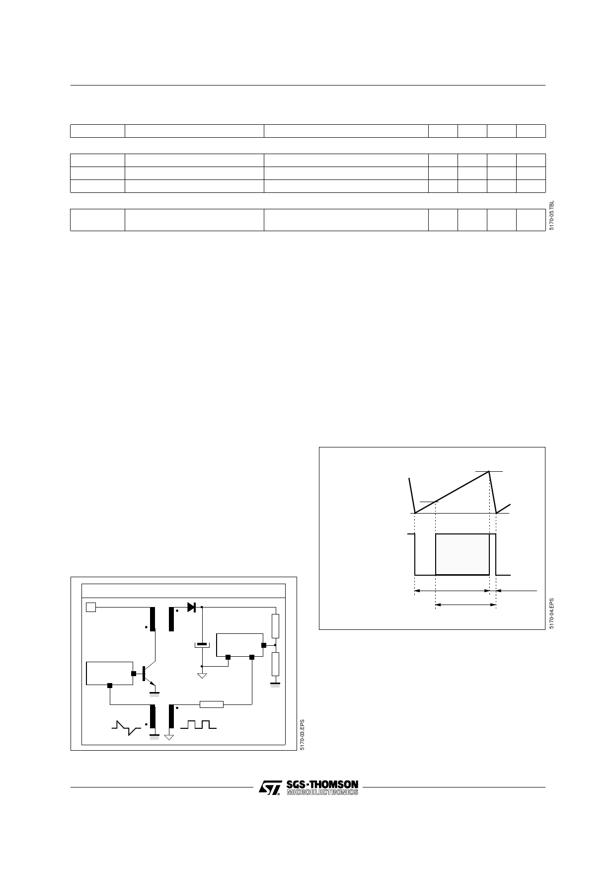
ASYNCHRONIZED MODE (Figure 2)
The regulated voltage image is compared to 2V
vol-tage reference. The error voltage amplifier out-
put and the RC oscillator voltage ramp are applied
to the internal Pulse Width Modulator Inputs.
The PWM logic Output is connected to a logic bloc
which behaves like a RS latch, sets by the PWM
output and resets when Ct downloading occurs.
Finally, the push-pull output bloc delivers square
wave signal whom output leading edge occurs
during Ct uploading time, and output trailing edge
at Ct downloading time end. The duty cycle is
limited to 75% of oscillator period as maximum
value and to Ct downloading time/oscillator period
as minimum value (Figure 2).
Figure 2
PRINCIPLE OF OPERATION
The TEA5170 sends pulses continuously to the
slave circuit in order to insure a proper behaviour
of the primary side.
- According to this, the output duty cycle is varying
between DON (min.) (0.05) and DON (max.) (0.75) :
then even in case of open load, pulses are still
sent to the slave circuit.
Figure 1 : Basic Concept
MASTER-SLAVE ARCHITECTURE
V2
OSCILLATOR RAMP
Vt max.
V1
POWER OUTPUT
T1
Ton max.
T2 = Ton min.
SLAVE
CIRCUIT
4/9
MASTER
CIRCUIT
PWM
SYNCHRONIZED MODE (see Figure 3)
The TEA5170 will enter the Synchronized Mode
when it receives one pulse through Rt during Ct
discharge.
At that time Ct charging current will be multiplied
by 0.75 and period will increase up to To x 1.26.
A pulse occuring during the synchro window, com-
mands the Ct downloading. If none, the TEA5170
will return to normal mode at the end of the period.
Share Link: 