PI6C133-03V 데이터 시트보기 (PDF) - Pericom Semiconductor
부품명
상세내역
일치하는 목록
PI6C133-03V Datasheet PDF : 15 Pages
| |||
PI6C133-03
133 MHz Clock Generation
1122334455667788990011223344556677889900112233445566778899001122112233445566778899001122334455667788990011223344556677889900112211223344556677889900112233445566778899001122334455667788990011221122334455667788f99o00r1122P3344e55n6677t88i99u00m11223344I55I66/77I88I99I0011P22r1122o33c44e5566s77s88o99r0011s22
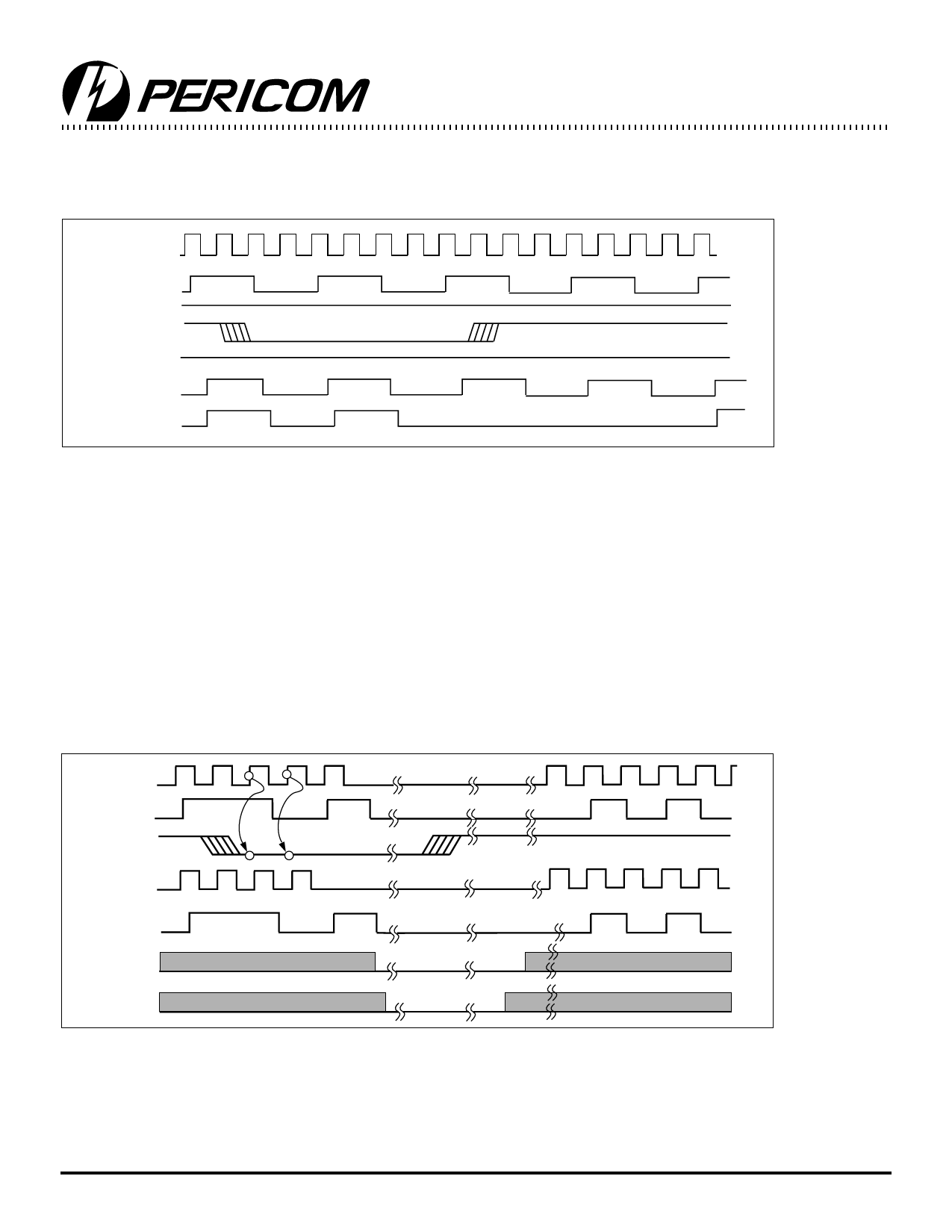
PCISTOP# is an input to the clock synthesizer and is made synchronous to the clock driver PCI_F output. It is used to turn
off the PCI clocks for low-power operation. PCI clocks are required to be stopped in a low state and started such that a full high pulse
width is guaranteed. ONLY one rising edge of PCI_F is needed after the clock control logic switched for the PCI outputs to become
enabled/disabled.
CPUCLK
(internal)
PCICLK
(internal)
CPUSTOP#=H
PCISTOP#
PWRDWN#=H
PCICLK_F
(external)
PCICLK
(external)
Notes:
PI6C133-03 PCISTOP# Timing Diagram
1. All internal timing is referenced to the CPUCLK
2. PCISTOP# signal is an input signal which is made synchronous to PCI_F output.
3. Internal means inside the chip.
4. All other clocks continue to run undisturbed.
5. PWRDWN# and CPUSTOP# are shown in a high state.
6. Diagrams shown with respect to 133 MHz. Similar operation when CPU is 100 MHz.
The power-down selection is used to put the part into a very low power state without turning off the power to the part. PWRDWN# is an
asynchronous active low input. The signal needs to be synchronized internal to the device prior to powering down the clock synthesizer.
PWRDWN# is an asynchronous function for powering up the system. Internal clocks are not running after the device is put in power down.
When PWRDWN# is active low all clocks need to be driven to a low value and held prior to turning off the VCOs and the crystal. The
power-up latency is less than 3ms. The power-down latency is short and conforms to the sequence requirements shown below. PCISTOP#
and CPUSTOP# are considered to be dont cares during power-down operations. REF and 48 MHz clocks are expected to be stopped
in the LOW state as soon as possible. Owing to the state of internal logic stopping and holding REF clock outputs in the LOW state, more
than one clock cycle may be required to complete.
CPUCLK
(internal)
PCICLK
(internal)
PWRDWN#
CPUCLK
(external)
PCICLK
(external)
VCO
Crystal
Notes:
PI6C133-03 PWRDWN# Timing Diagram
1. All internal timing is referenced to the CPUCLK
2. Internal means inside the chip.
3. PWRDWN# is an asynchronous input and metstable conditions could exist.
This signal is required to be synchronized inside the part.
4. The shaded sections on the VCO and the crystal signals indicate an active clock.
5. Diagrams shown with respect to 133 MHz. Similar operation when CPU is 100 MHz.
355
PS8415
07/23/99
Share Link: 