PI6C133-03V 데이터 시트보기 (PDF) - Pericom Semiconductor
부품명
상세내역
일치하는 목록
PI6C133-03V Datasheet PDF : 15 Pages
| |||
PI6C133-03
133 MHz Clock Generation
1122334455667788990011223344556677889900112233445566778899001122112233445566778899001122334455667788990011223344556677889900112211223344556677889900112233445566778899001122334455667788990011221122334455667788f99o00r1122P3344e55n6677t88i99u00m112233I4455I66/77I88I99I0011P22r1122o33c44e5566s77s88o99r0011s22
PI6C133-03 Power Management Requirements
Signal
Signal State
Latency
No. of rising edges of PCICLK
0 (Disabled)
1
CPUSTOP#
1 (Enabled)
1
0 (Disabled)
1
PCISTOP#
1 (Enabled)
1
PWRDWN#
1 (Normal Operation)
0 (Power Down)
3ms
2 max.
Notes:
1. Clock on/off latency is defined in the number of rising edges of free running PCICLKs
between the clock disable goes low/high to the first valid clock comes out of the device.
2. Power up latency is when PWRDWN# goes inactve (high) to when the first valid clocks
are driven from the device.
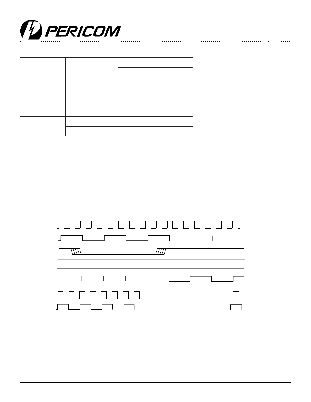
CPUSTOP# is an input to the clock synthesizer. It is used to turn off the CPU and 3V66 clocks for low power operation. CPUSTOP#
is asserted asynchronously by the external clock control logic with the rising edge of the free running PCI clock (and hence CPU clock)
and must be internally synchronized to the external PCI_F output. All other clocks will continue to run while the CPU clocks are disabled.
The CPU clocks must always be stopped in a low state and started in such a manner as to guarantee that the high pulse width is a full pulse.
ONLY one rising edge of the PCI_F is allowed after the clock control logic switched for both the CPU and 3V66 outputs to become
enabled/disabled.
CPUCLK
(internal)
PCICLK
(internal)
CPUSTOP#
PCISTOP#=H
PWRDWN#=H
PCI_REF
(external)
CPUCLK
(external)
3V66
(external)
PI6C133-03 CPUSTOP# Timing Diagram
Notes:
1. All internal timing is referenced to the CPUCLK
2. The internal label means inside the chip and is a reference only. This in fact may not be the way that the control is designed.
3. CPUSTOP# signal is an input signal that must be made synchronous to free running PCI_F
4. 3V66 clocks also stop/start before
5. PWRDWN# and PCISTOP# are shown in a high state.
6. Diagrams shown with respect to 133 MHz. Similar operation when CPU is 100 MHz.
354
PS8415
07/23/99
Share Link: 