PI6C102-16BH 데이터 시트보기 (PDF) - Pericom Semiconductor
부품명
상세내역
일치하는 목록
PI6C102-16BH Datasheet PDF : 12 Pages
| |||
PI6C102-16 111222333444555666777888999000111222333444555666777888999000111222333444555666777888999000111222111222333444555666777888999000111222333444555666777888999000111222333444555666777888999000111222111222333444555666777888999000111222333444555666777888999000111222333444555666777888999000111222111222333444555666777888999000111222333444555666777888999000111222333444555666777888999000111222111222333444555666777888999000111222
Spread Spectrum Clock Synthesizer
for Mobile Pentium II
Features
· 100 MHz or 66.6 MHz operation
· Two copies of CPU clock with VDD of 2.5V
· High drive option to support modular mobile CPUs
· Six copies of PCI clock, (synchronous with CPU clock) 3.3V
· One copy of Ref. Clock @ 14.31818 MHz (3.3VTTL)
· One copy of 48 MHz Clock (3.3V)
· Low cost 14.31818 MHz crystal oscillator input
· Power management control
· Isolated core VDD, VSS pins for noise reduction
· Down spread (–16) or center spread spectrum (–16B) options
· 28-pin SSOP package (H)
Description
Pericom Semiconductor’s PI6C clock series are produced using the
company’s advanced submicron CMOS technology, achieving
industry leading speed.
PI6C102-16 is a high-speed, low-noise, clock generator that works
with Pericom’s PI6C18x clock buffer to meet all clock needs for
Mobile Intel Architecture platforms. CPU and chipset clock fre-
quencies of 66.6 MHz and 100 MHz are supported.
Split supplies of 3.3V and 2.5V are used. The 3.3V power supply
powers a portion of the I/O and the core. The 2.5V is used to power
the remaining outputs. 2.5V signaling follows JEDEC standard
8-X. Power sequencing of the 3.3V and 2.5V supplies is not
required.
An asynchronous PWRDWN# signal may be used to orderly power
down (or up) the system.
PI6C102-16 is –0.6% down spread, where as PI6C102-16B is
±0.75% center spread.
PI6C102-16D is the high drive version of PI6C102-16
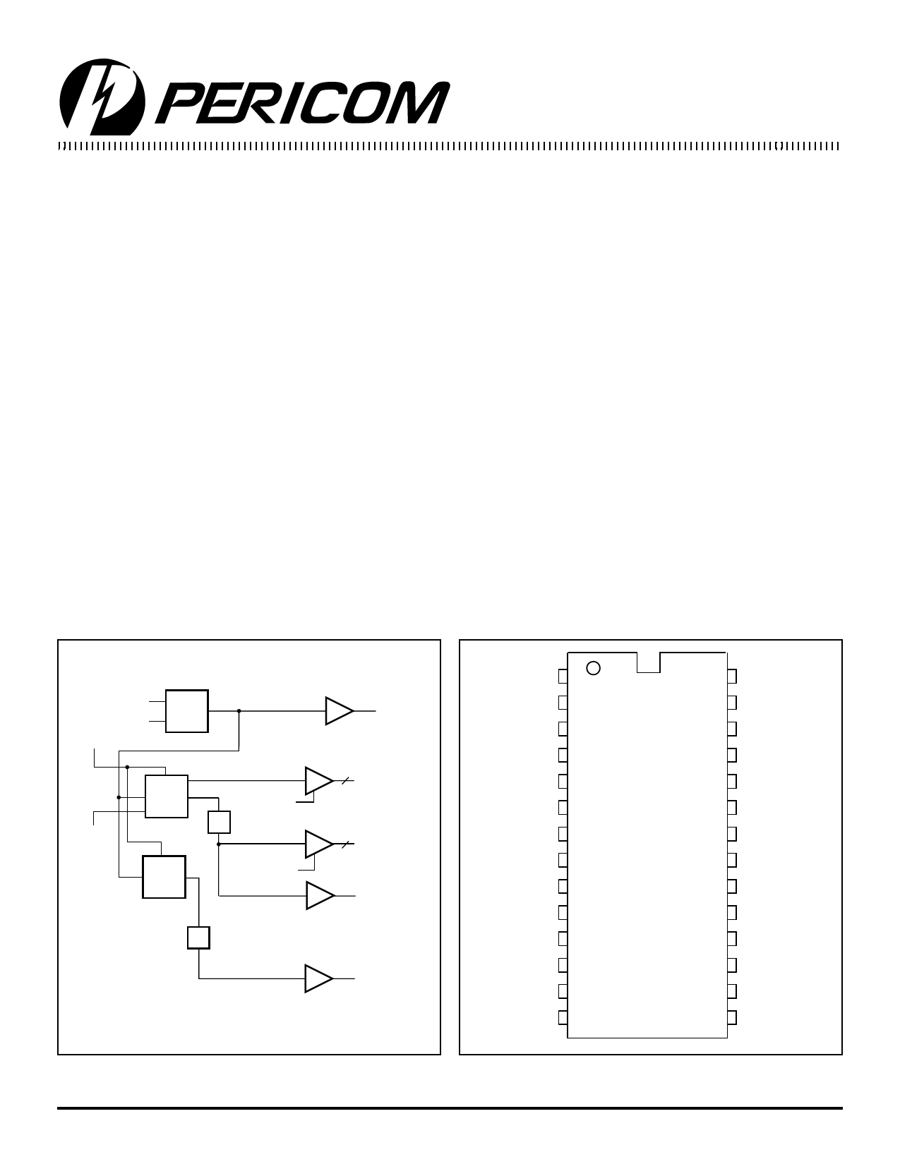
Block Diagram
Pin Configuration
XTAL_IN REF
XTAL_OUT OSC
PWRDWN#
SEL
100/66#
PLL1
CPUSTOP#
Div
PLL2
PCISTOP#
÷2
REF
2 CPUCLK[0:1]
5 PCICLK[1:5]
PCICLK_F
48MHz
XTAL_IN 1
XTAL_OUT 2
VSS 3
PCICLK_F 4
PCICLK1 5
VDD 6
PCICLK2 7
PCICLK3 8
VDD 9
PCICLK4 10
PCICLK5 11
VSS 12
VDD 13
VSS 14
28-Pin
H
28 VSS
27 VDD
26 REF
25 VDD2
24 CPUCLK0
23 CPUCLK1
22 VSS2
21 VDD
20 VSS
19 PCISTOP#
18 CPUSTOP#
17 PWRDWN#
16 48MHz
15 SEL100/66#
1
P8399-1 06/11/99
Share Link: 