NJU6350 데이터 시트보기 (PDF) - Japan Radio Corporation
부품명
상세내역
일치하는 목록
NJU6350 Datasheet PDF : 9 Pages
| |||
NJU6350
2. Data writing operation
Data writing performs to set the system control data block ( 4 bits ) and the mode set data ( Oscillator output
control and Test mode set ) or the timer data block ( 8 bits, but only data of " Days of Week " is 4 bits ) to
NJU6350.
The CE terminal is set to " H ", and the data is written into the shift register in the NJU6350 from the DATA
terminal synchronizing with the rising edge of the clock signal input from the CLK terminal.
At first, System control data is written into NJU6350. The first 4 bits of them are effective. When the bit of
“ RW ” in System control data is “ 1 ”, the mode goes to writing. In the writing mode, the update of the timer is
stopped and the oscillator divider is cleared excepting for the Oscillation output set and Test mode set.
At second, Timer data is written into NJU6350. The last 8 bits of them are effective. ( In case of Days of week,
the last 4 bits are effective. )
The data order to write is LSB first.
The oscillator divider starts the operation when the CE signal is changed from “ H ” or “ L “.
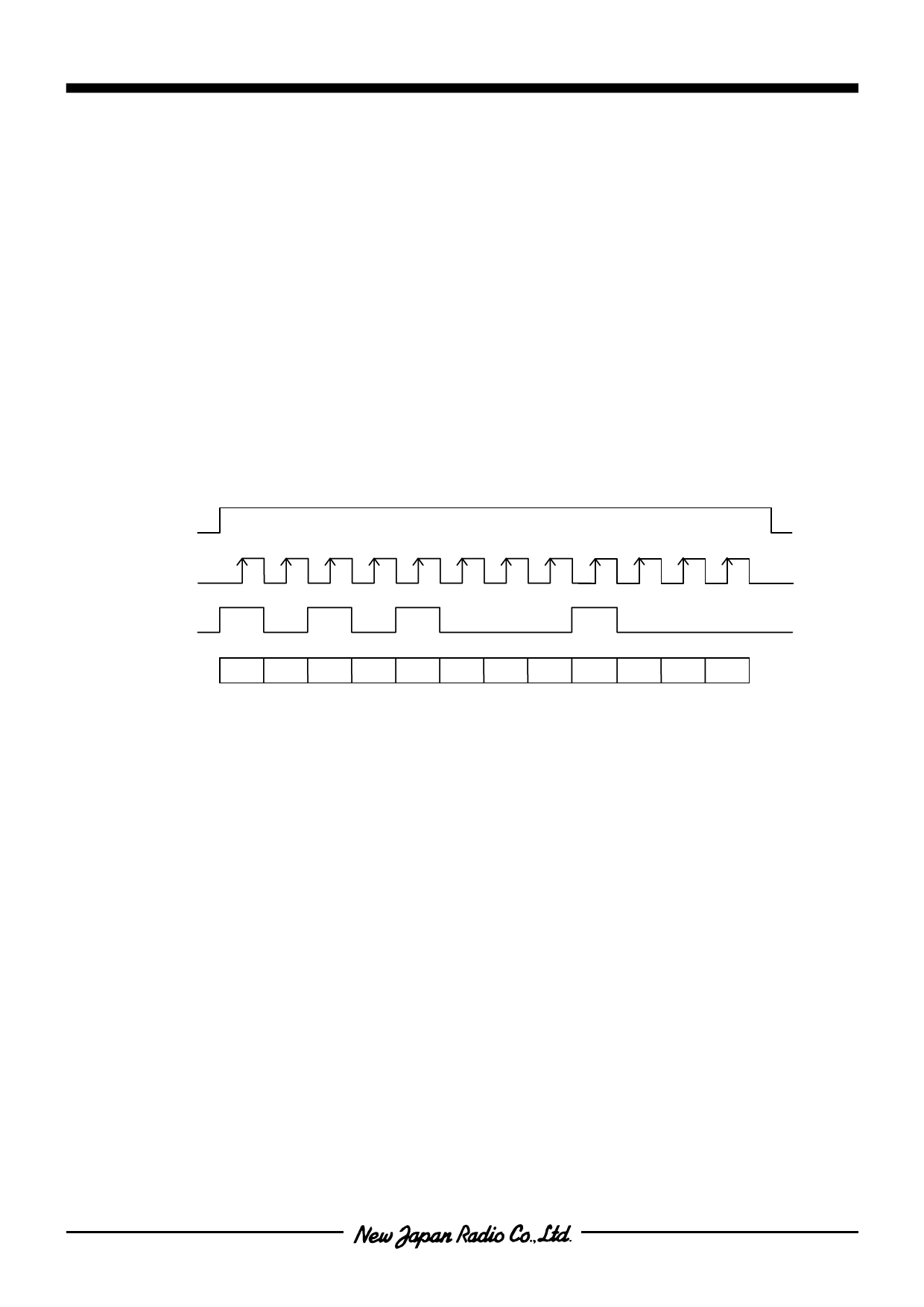
< Writing timer data >
In case of November
CE
1 2 3 4 5 6 7 8 9 10 11 12
CLK
Input data
DATA 1 0 1 0 1 0 0 0 1 0 0 0
RW C0 C1 C2 M0 M1 M2 M3 M4 0 0 0
(Note3) In case of over than 12 bits data, valid data is the first 4 bits as System control data and the last 8 bits
as Timer data. ( In case of Days of week, it is the last 4 bits is effective. )
3. Data reading operation
Data reading performs to send the Timer data ( 8 bits, but only data of " Days of Week " is 4 bits )
corresponding the system control data from NJU6350 after the system control data ( 4 bits ) is set to NJU6350.
The CE terminal is set to " H ", and the System control data are written into the shift register in the NJU6350
from the DATA terminal synchronized with the rising edge of the clock signal input from the CLK terminal.
At first, System control data is written into NJU6350. The first 4 bits of them are effective. When the bit of
“ RW ” in System control data ( Except the “ 0,0,0,0 ” data. ) is “ 0 ” the mode goes to reading. When the falling
edge of the clock signal is input from the CLK terminal just after the recognition of reading mode, the DATA
terminal is changed from Input to Output. The first 8 bits of Read data is effective. ( In case of Days of week,
the first 4 bits is effective. ) After the falling edge of the CE terminal, the DATA terminal is changed from Output
to Input. The data order to read is LSB first.
(Note4) In case of counting the timer up during the data reading.
The difference between the read out data of timer and the actual timer data is sometimes occurred. ( The
difference range depend on condition. )
In case of “ 99.12.31.Sat.23:59:59 ” at the current time, the update is operated immediately after year but
“ 99 ” is read out, the data is the result of reading operation is “ 99.1.1.Sun.0:0:0 ” instead of the true data
“ 00.1.1.Sun.0:0:0 ”.
Share Link: 