NJU6350 데이터 시트보기 (PDF) - Japan Radio Corporation
부품명
상세내역
일치하는 목록
NJU6350 Datasheet PDF : 9 Pages
| |||
NJU6350
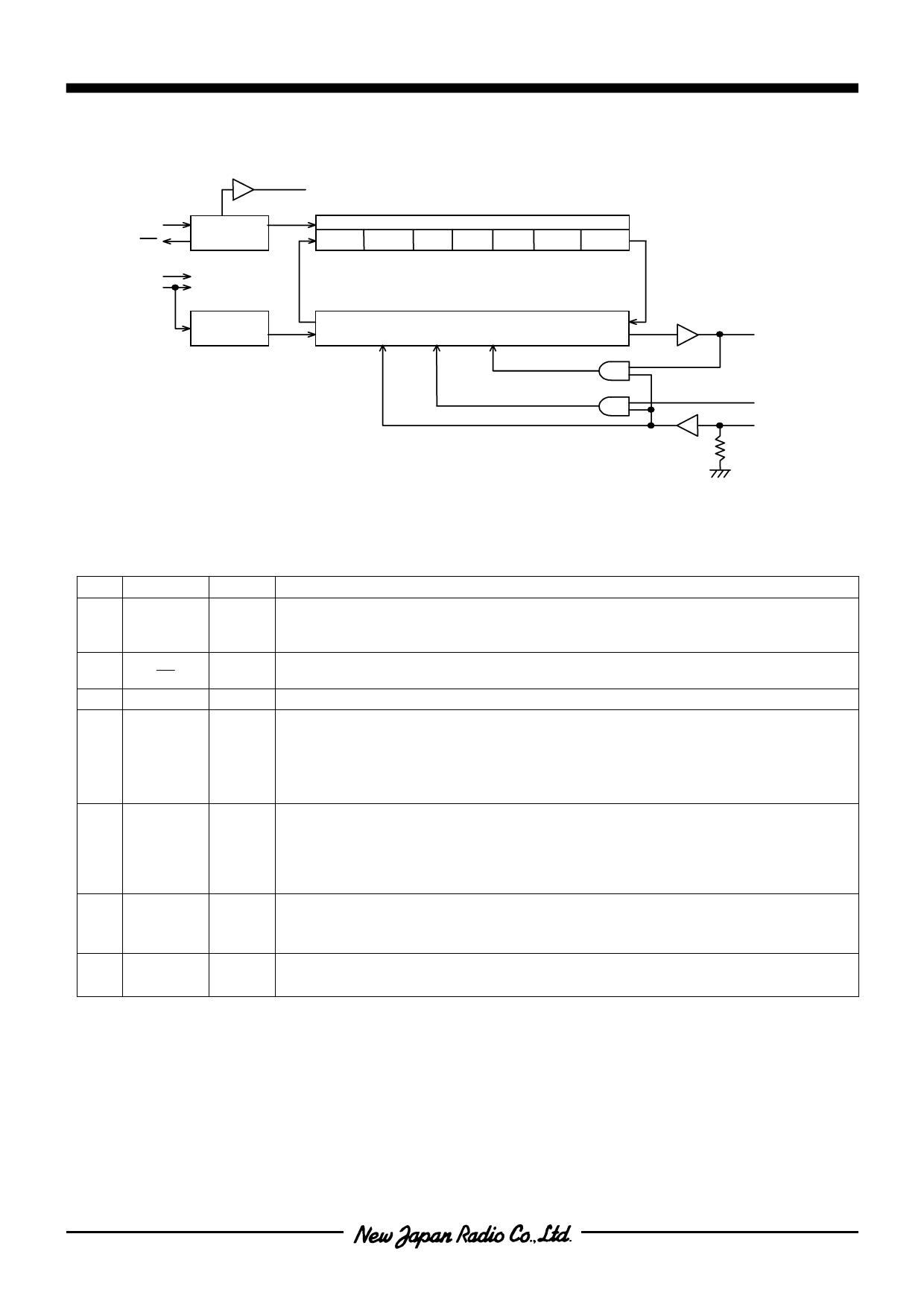
s BLOCK DIAGRAM
XT
Oscillator
XT
Divider
VSS
VDD
Low Voltage
Detector
Fout
Timer Counter
sec. min. hour day date month year
Controller
DATA
CLK
CE
s TERMINAL DESCRIPTION
No. SYMBOL
1
Fout
2
XT
3
XT
4
VSS
5
CE
6
CLK
7
DATA
8
VDD
I/O
O
I
O
Power
I
I
I/O
Power
FUNCTION
Oscillator output terminal.
ON :It outputs oscillator signal , frequency 32.768kHz.
OFF :It is in high impedance status.
Quartz crystal connect terminal ( f = 32.768kHz ).
GND
Chip enable terminal ( With pull-down resistor ).
" H " : Data input/output available
" L " : Data terminal is in high impedance status.
When the data input/output is executed consequently, the CE terminal should be
set to " L " level at the data transmission interval.
Clock terminal.
The Data Input/Output is synchronized by this clock. When the CE terminal is "L",
the data input is not available.
When the CE signal which is raising edge or falling edge, the CLK signal should
be fixed to " L ".
Serial timer data input/output terminal.
This terminal is switched to input or output by system control data. (Defult : input)
When the CE terminal is set to " L ", the data terminal is high impedance.
Power supply
The rising time of VDD should be less than 10mS.
Share Link: 