HS-82C37ARH(1995) 데이터 시트보기 (PDF) - Intersil
부품명
상세내역
일치하는 목록
HS-82C37ARH Datasheet PDF : 29 Pages
| |||
HS-82C37ARH
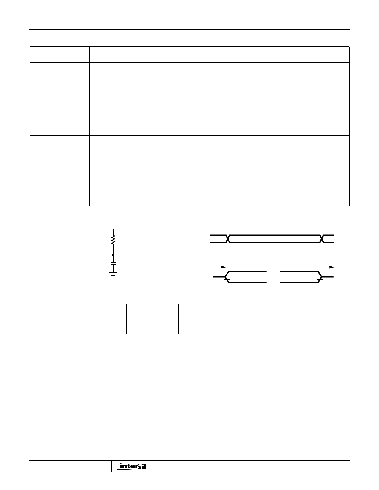
Pin Descriptions (Continued)
PIN
SYMBOL NUMBER TYPE
DESCRIPTION
A4-A7
37-40
O Address: The four most significant address lines are three-state outputs and provide 4 bits of address.
These lines are enabled only during the Active cycle.
HRQ
10
O Hold Request: The Hold Request (HRQ) output is used to request control of the system bus. When a
DREQ occurs and the corresponding mask bit is clear, or a software DMA request is made, the HS-
82C37ARH issues HRQ. The HLDA signal then informs the controller when access to the system bus-
ses is permitted. For stand-alone operation where the HS-82C37ARH always controls the busses, HRQ
may be tied to HLDA. This will result in one S0 state before the transfer.
DACK0- 14,15, 24,
DACK3
25
O DMA Acknowledge: DMA acknowledge is used to notify the individual peripherals when one has been
granted a DMA cycle. The sense of these lines is programmable. Reset initializes them to active low.
AEN
9
O Address Enable: Address Enable enables the 8-bit latch containing the upper 8 address bits onto the
system address bus. AEN can also be used to disable other system bus drivers during DMA transfers.
AEN is active HIGH.
ADSTB
8
O Address Strobe: This is an active high signal used to control latching of the upper address byte. It will
drive directly the strobe input of external transparent octal latches, such as the 82C82. During block op-
erations, ADSTB will only be issued when the upper address byte must be updated, thus speeding op-
eration through elimination of S1 states. (See Note 2).
MEMR
3
O Memory Read: The Memory Read signal is an active low three-state output used to access data from
the selected memory location during a DMA Read or a Memory-to-Memory transfer.
MEMW
4
O Memory Write: The Memory Write is an active low three-state output used to write data to the selected
memory location during a DMA Write or a Memory-to-Memory transfer.
NC
5
No connect. Pin 5 is open and should not be tested for continuity.
Spec Number 518058
921
Share Link: 