HS-80C86RH 데이터 시트보기 (PDF) - Intersil
부품명
상세내역
일치하는 목록
HS-80C86RH Datasheet PDF : 29 Pages
| |||
HS-80C86RH
into relocatable areas of similar characteristics and by
automatically selecting segment registers, programs are
shorter, faster and more structured. (See Table 1).
Word (16-bit) operands can be located on even or odd
address boundaries and are thus not constrained to even
boundaries as is the case in many 16-bit computers. For
address and data operands, the least significant byte of the
word is stored in the lower valued address location and the
most significant byte in the next higher address location. The
BlU automatically performs the proper number of memory
accesses, one if the word operand is on an even byte
boundary and two if it is on an odd byte boundary. Except for
the performance penalty, this double access is transparent to
the software. The performance penalty does not occur for
instruction fetches; only word operands.
Physically, the memory is organized as a high bank (D15-
D6) and a low bank (D7-D0) of 512K bytes addressed in
parallel by the processor’s address lines.
Byte data with even addresses is transferred on the D7-D0
bus lines while odd addressed byte data (A0 HIGH) is
transferred on the D15-D6 bus lines. The processor provides
two enable signals, BHE and A0, to selectively allow reading
from or writing into either an odd byte location, even byte
location, or both. The instruction stream is fetched from
memory as words and is addressed internally by the
processor at the byte level as necessary.
In referencing word data, the BlU requires one or two
memory cycles depending on whether the starting byte of
the word is on an even or odd address, respectively.
Consequently, in referencing word operands performance
can be optimized by locating data on even address
boundaries. This is an especially useful technique for using
the stack, since odd address references to the stack may
adversely affect the context switching time for interrupt
processing or task multiplexing.
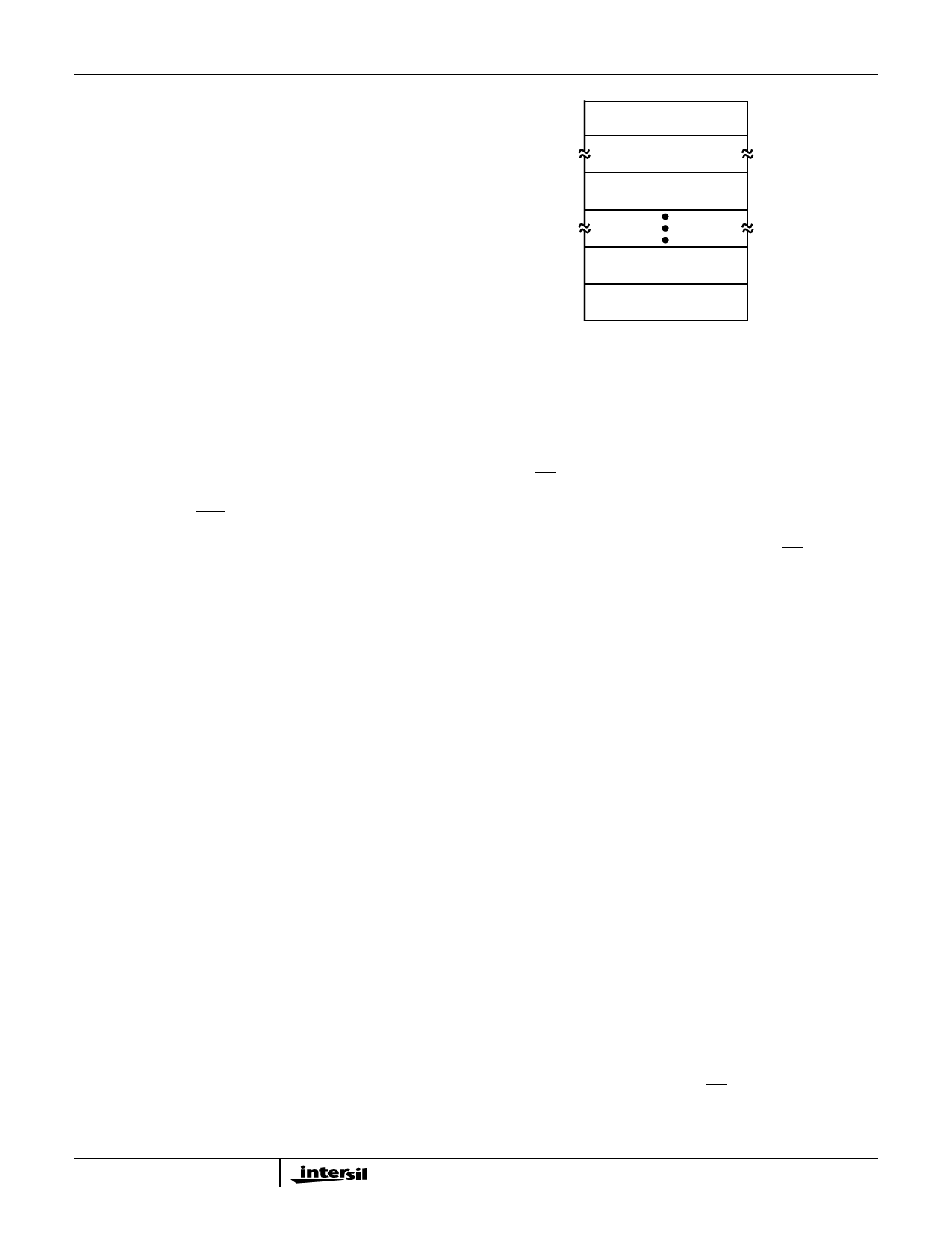
Certain locations in memory are reserved for specific CPU
operations (See Figure 10). Locations from address FFFF0H
through FFFFFH are reserved for operations including a
jump to the initial program loading routine. Following RESET,
the CPU will always begin execution at location FFFF0H
where the jump must be located. Locations 00000H through
003FFH are reserved for interrupt operations. Each of the
256 possible interrupt service routines is accessed through
its own pair of 16-bit pointers - segment address pointer and
offset address pointer. The first pointer, used as the offset
address, is loaded into the 1P and the second pointer, which
designates the base address is loaded into the CS. At this
point program control is transferred to the interrupt routine.
The pointer elements are assumed to have been stored at
the respective places in reserved memory prior to
occurrence of interrupts.
RESET BOOTSTRAP
PROGRAM JUMP
FFFFFH
FFFFOH
INTERRUPT POINTER
FOR TYPE 255
3FFH
3FCH
7H
INTERRUPT POINTER
FOR TYPE 1
4H
INTERRUPT POINTER
3H
FOR TYPE 0
0H
FIGURE 10. RESERVED MEMORY LOCATIONS
Minimum and Maximum Operation Modes
The requirements for supporting minimum and maximum
HS-80C86RH systems are sufficiently different that they
cannot be met efficiently using 40 uniquely defined pins.
Consequently, the HS-80C86RH is equipped with a strap pin
(MN/MX) which defines the system configuration. The
definition of a certain subset of the pins changes, dependent
on the condition of the strap pin. When the MN/MX pin is
strapped to GND, the HS-80C86RH defines pins 24 through
31 and 34 in maximum mode. When the MN/MX pin is
strapped to VDD, the HS-80C86RH generates bus control
signals itself on pins 24 through 31 and 34.
Bus Operation
The HS-80C86RH has a combined address and data bus
commonly referred to as a time multiplexed bus. This
technique provides the most efficient use of pins on the
processor while permitting the use of a standard 40-lead
package. This “local bus” can be buffered directly and used
throughout the system with address latching provided on
memory and I/O modules. In addition, the bus can also be
demultiplexed at the processor with a single set of 82C82
latches if a standard non-multiplexed bus is desired for
the system.
Each processor bus cycle consists of at least four CLK
cycles. These are referred to as T1, T2, T3 and T4 (see
Figure 11). The address is emitted from the processor
during T1 and data transfer occurs on the bus during T3 and
T4. T2 is used primarily for changing the direction of the bus
during read operations. In the event that a “NOT READY”
indication is given by the addressed device, “Wait” states
(TW) are inserted between T3 and T4. Each inserted wait
state is the same duration as a CLK cycle. Idle periods occur
between HS-80C86RH driven bus cycles whenever the
processor performs internal processing.
During T1 of any bus cycle, the ALE (Address Latch Enable)
signal is emitted (by either the processor or the 82C88 bus
controller, depending on the MN/MX strap). At the trailing
edge of this pulse, a valid address and certain status
information for the cycle may be latched.
17
Share Link: 