HS-80C86RH(1995) 데이터 시트보기 (PDF) - Intersil
부품명
상세내역
일치하는 목록
HS-80C86RH Datasheet PDF : 37 Pages
| |||
HS-80C86RH
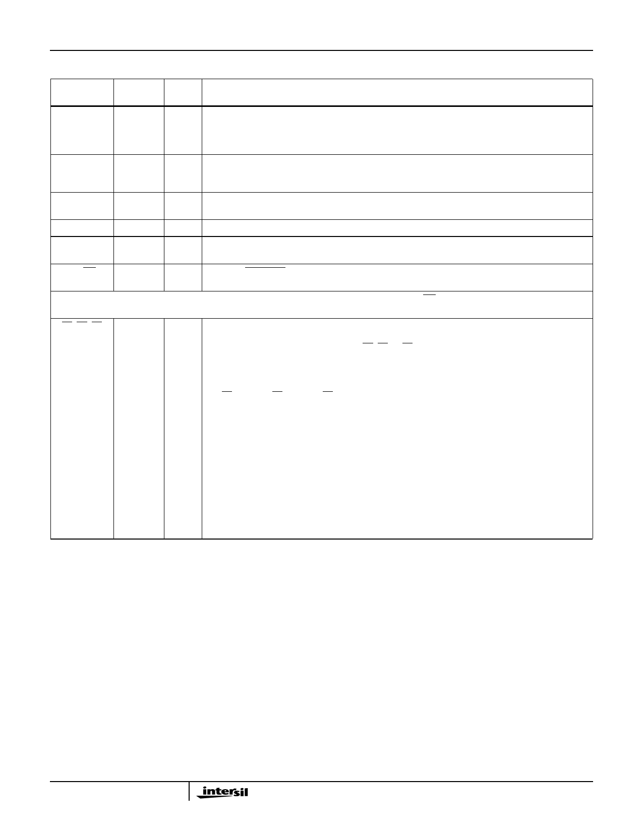
Pin Description (Continued)
SYMBOL
PIN
NUMBER TYPE
DESCRIPTION
RESET
21
I
RESET: causes the processor to immediately terminate its present activity. The signal must
change from LOW to HIGH and remain active HIGH for at least 4 CLK cycles. It restarts
execution, as described in the Instruction Set description, when RESET returns LOW. RESET is
internally synchronized.
CLK
19
I
CLOCK: provides the basic timing for the processor and bus controller. It is asymmetric with a
33% duty cycle to provide optimized internal timing.
VDD
40
VDD: +5V power supply pin. A 0.1µF capacitor between pins 20 and 40 is recommended for
decoupling.
GND
1, 20
GND: Ground. Note: both must be connected. A 0.1µF capacitor between pins 1 and 20 is
recommended for decoupling.
MN/MX
33
I
MINIMUM/MAXIMUM: Indicates what mode the processor is to operate in. The two modes are
discussed in the following sections.
The following pin function descriptions are for the HS-80C86RH system in maximum mode (i.e., MN/MX = GND). Only the pin functions
which are unique to maximum mode are described below.
S0, S1, S2
26-28
O
STATUS: is active during T4, T1 and T2 and is returned to the passive state (1,1,1) during T3
or during TW when READY is HIGH. This status is used by the 82C88 Bus Controller to generate
all memory and I/O access control signals. Any change by S2, S1, or S0 during T4 is used to
indicate the beginning of a bus cycle, and the return to the passive state in T3 or TW is used to
indicate the end of a bus cycle. These status lines are encoded. These signals are held at a high
impedance logic one state during “grant sequence”.
S2
S1
S0
0
0
0
Interrupt Acknowledge
0
0
1
Read I/O Port
0
1
0
Write I/O Port
0
1
1
Halt
1
0
0
Code Access
1
0
1
Read Memory
1
1
0
Write Memory
1
1
1
Passive
RQ/GT0
RQ/GT1
31, 30
I/O REQUEST/GRANT: pins are used by other local bus masters to force the processor to release the
local bus at the end of the processor’s current bus cycle. Each pin is bidirectional with RQ/GT0 hav-
ing higher priority than RQ/GT1. RQ/GT has an internal pull-up bus hold device so it may be left
unconnected. The request/grant sequence is as follows (see RQ/GT Sequence Timing.)
1. A pulse of 1 CLK wide from another local bus master indicates a local bus request (“hold”) to
the HS-80C86RH (pulse 1).
2. During a T4 or T1 clock cycle, a pulse 1 CLK wide from the HS-80C86RH to the requesting
master (pulse 2) indicates that the HS-80C86RH has allowed the local bus to float and that
it will enter the “grant sequence” state at the next CLK. The CPU’s bus interface unit is dis-
connected logically from the local bus during “grant sequence”.
3. A pulse 1 CLK wide from the requesting master indicates to the HS-80C86RH (pulse 3) that
the “hold” request is about to end and that the HS-80C86RH can reclaim the local bus at the
next CLK. The CPU then enters T4 (or T1 if no bus cycles pending).
Each Master-Master exchange of the local bus is a sequence of 3 pulses. There must be
one idle CLK cycle after each bus exchange. Pulses are active low.
If the request is made while the CPU is performing a memory cycle, it will release the local
bus during T4 of the cycle when all the following conditions are met:
1. Request occurs on or before T2.
2. Current cycle is not the low byte of a word (on an odd address).
3. Current cycle is not the first acknowledge of an interrupt acknowledge sequence.
4. A locked instruction is not currently executing.
If the local bus is idle when the request is made the two possible events will follow:
1. Local bus will be released during the next cycle.
2. A memory cycle will start within 3 CLKs. Now the four rules for a currently active memory
cycle apply with condition number 1 already satisfied.
Spec Number 518055
860
Share Link: 