SL4029BN 데이터 시트보기 (PDF) - System Logic Semiconductor
부품명
상세내역
일치하는 목록
SL4029BN Datasheet PDF : 8 Pages
| |||
SL4029B
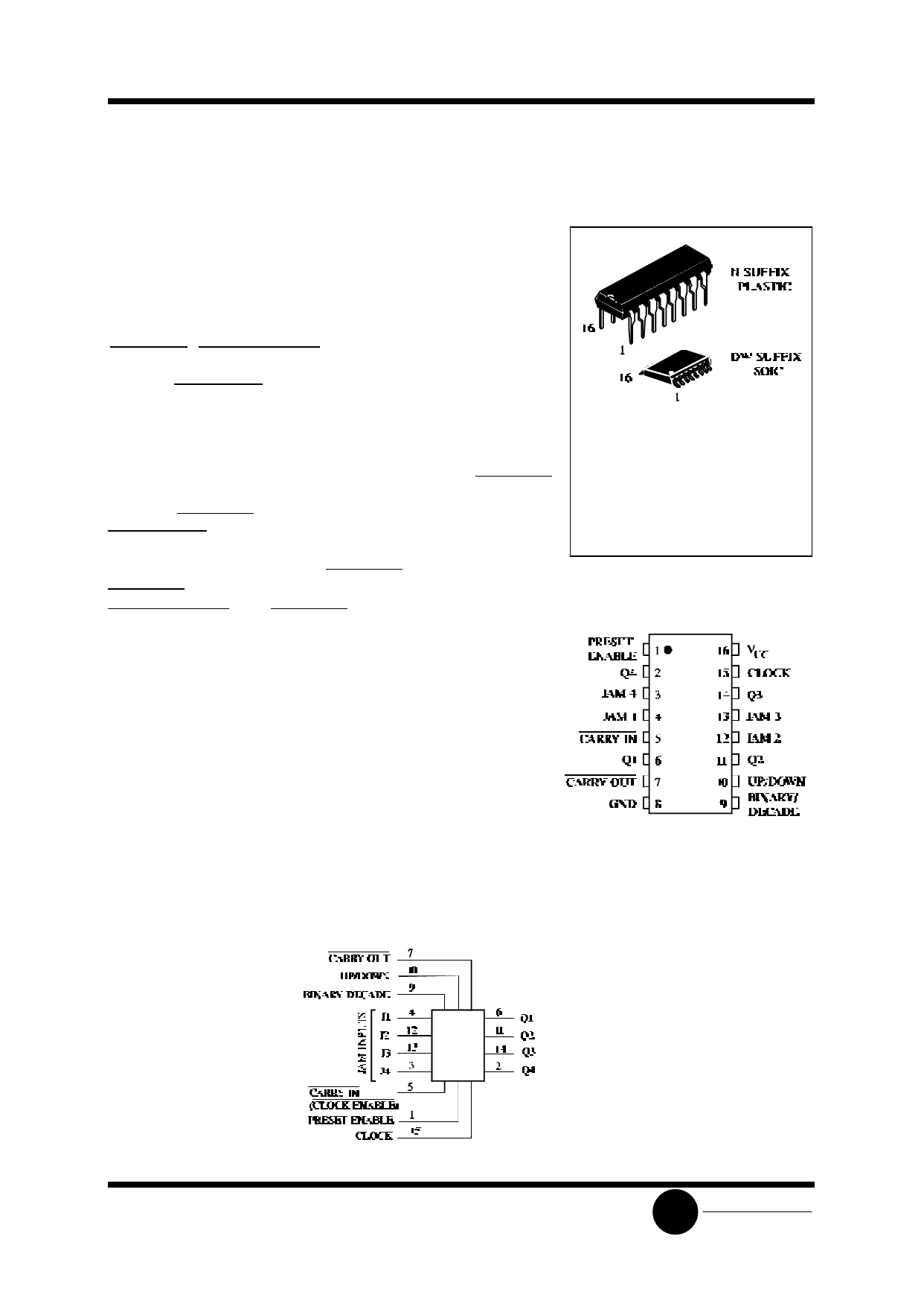
Presettable Up/Down Counter
High-Voltage Silicon-Gate CMOS
The SL4029B consists of a four-stage binary or BCD-decade
up/down counter with provisions for look-ahead carry in both counting
modes. The inputs consists of a single CLOCK,
CARRY IN,(CLOCK ENABLE), BINARY/DECADE, UP/DOWN,
PRESET ENABLE, and four individual JAM signals. Q1, Q2, Q3, Q4 and
a CARRY OUT signal are provided as outputs.
A high PRESET ENABLE signal allows information on the JAM
INPUTS to preset the counter to any state asynchronously with the
clock. A low on each JAM line, when the PRESET-ENABLE signal is
high, resets the counter to its zero count. The counter is advanced one
count at the positive transition of the clock when the CARRY IN and
PRESET ENABLE signals are low. Advancement is inhibited when the
CARRY IN or PRESET ENABLE signals are high. The CARRY OUT
signal is normally high and goes low when the counter reaches its
maximum count in the UP mode or the minimum count in the DOWN
mode provided the CARRY IN signal is low. The CARRY IN signal
in the low state can thus be considered a CLOCK ENABLE. The
CARRY IN terminal must be connected to GND when not in use.
Binary counting is accomplished when the BINARY/DECADE
input is high; the counter counts in the decade mode when the
BINARY/DECADE input is low. The counter counts up when the
UP/DOWN input is high, and down when the UP/DOWN input is
low.
Parallel clocking provides synchronous control and hence faster
response from all counting outputs. Ripple-clocking allows for
longer clock input rise and fall times.
• Operating Voltage Range: 3.0 to 18 V
• Maximum input current of 1 µA at 18 V over full package-
temperature range; 100 nA at 18 V and 25°C
• Noise margin (over full package temperature range):
1.0 V min @ 5.0 V supply
2.0 V min @ 10.0 V supply
2.5 V min @ 15.0 V supply
LOGIC DIAGRAM
ORDERING INFORMATION
SL4029BN Plastic
SL4029BDW SOIC
TA = -55° to 125° C for all packages
PIN ASSIGNMENT
PIN 16=VCC
PIN 8= GND
SLS
System Logic
Semiconductor
Share Link: 