AD7545BN(1997) 데이터 시트보기 (PDF) - Intersil
부품명
상세내역
일치하는 목록
AD7545BN Datasheet PDF : 7 Pages
| |||
AD7545
Electrical Specifications TA = See Note 2, VREF = +10V, VOUT1 = 0V, AGND = DGND, Unless Otherwise Specified (Continued)
PARAMETER
TEST CONDITIONS
VDD = +5V
MIN TYP MAX
VDD = +15V
MIN TYP MAX
REFERENCE INPUT
Input Resistance (Pin 19 to GND) Input Resistance
TC = -300ppm/oC (Typ)
7
-
-
7
-
-
Typical Input Resistance = 11kΩ
-
-
25
-
-
25
DIGITAL INPUTS
Input High Voltage, VIH
Input Low Voltage, VIL
Input Current, IIN
VIN = 0 or VDD (Note 7)
Input Capacitance
DB0 - DB11
VIN = 0 (Note 4)
WR, CS
VIN = 0 (Note 4)
SWITCHING CHARACTERISTICS (Note 4)
2.4
-
-
-
-
13.5
-
-
0.8
-
-
1.5
±1
-
±10
±1
-
±10
-
-
7
-
-
7
-
-
20
-
-
20
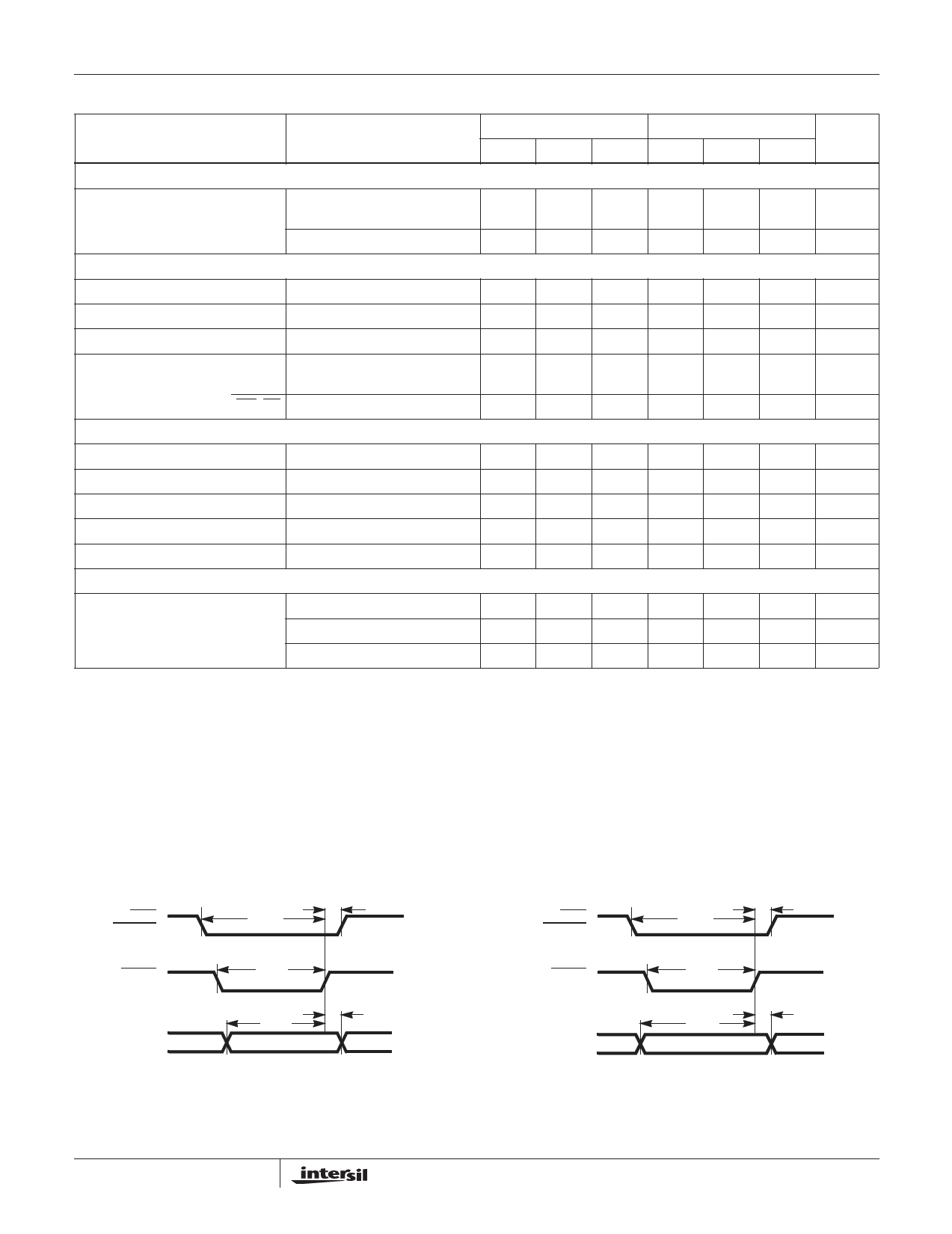
Chip Select to Write Setup Time, tCS See Figure 1
380
200
-
200
120
-
Chip Select to Write Hold Time, tCH See Figure 1
0
-
-
0
-
-
Write Pulse Width, tWR
tCS ≥ tWR, tCH ≥ 0, See Figure 1 400
175
-
240
100
Data Setup Time, tDS
See Figure 1
210
100
-
120
60
-
Data Hold Time, tDH
See Figure 1
10
-
-
10
-
-
POWER SUPPLY CHARACTERISTICS
IDD
All Digital Inputs VIL or VIH
-
-
2
-
All Digital Inputs 0V or VDD
-
100
500
-
All Digital Inputs 0V or VDD
-
10
-
-
NOTES:
2. Temperature Ranges as follows: J, K versions: 0oC to 70oC
A, B versions: -20oC to 85oC
S version: -55oC to 125oC
TA = 25oC for TYP Specifications. MIN and MAX are measured over the specified operating range.
3. This includes the effect of 5ppm maximum gain TC.
4. Parameter not tested. Parameter guaranteed by design, simulation, or characterization.
5. DB0 - DB11 = 0V to VDD or VDD to 0V in plastic and sidebraze package.
6. Feedthrough can be further reduced by connecting the metal lid on the ceramic package to DGND.
7. Logic inputs are MOS gates. Typical input current (25oC) is less than 1nA.
8. Typical values are not guaranteed but reflect mean performance specification.
Specifications subject to change without notice.
-
2
100
500
10
-
UNITS
kΩ
kΩ
V
V
µA (Max)
pF
pF
ns
ns
ns
ns
ns
mA
µA
µA
Timing Diagrams
CHIP
SELECT
WRITE
DATA IN
(DB0 - DB11)
tCH
tCS
tWR
tDH
tDS
DATA VALID
VDD
0
VDD
0
VDD
0
CHIP
SELECT
WRITE
DATA IN
(DB0 - DB11)
tCH
tCS
tWR
tDH
tDS
DATA VALID
VDD
0
VDD
0
VDD
0
FIGURE 1A. TYPICAL WRITE CYCLE
FIGURE 1B. PREFERRED WRITE CYCLE
FIGURE 1. WRITE CYCLE TIMING DIAGRAM
10-12
Share Link: 