LT1509 데이터 시트보기 (PDF) - Linear Technology
부품명
상세내역
일치하는 목록
LT1509 Datasheet PDF : 16 Pages
| |||
LT1509
PIN FUNCTIONS (For application help with the PFC portion of this chip, see the LT1248 data sheet)
RSET (Pin 15): A resistor from RSET to GND sets the
oscillator charging current and the maximum multiplier
output current which is used to limit the maximum line
current.
IM(MAX) = 3.75V/RSET
SS1 (Pin 16): Soft Start. SS1 is reset to zero for low VCC.
When VCC rises above lockout threshold, SS1 is released
to ramp up at a rate set by the internal 12µA current source
and an external capacitor. During this ramp up, PFC
reference voltage is equal to SS1 voltage. After SS1 rises
past 7.5V, reference voltage remains at 7.5V.
VCC (Pin 17): This is the supply for the chip. The LT1509
has two fast gate drivers required to fast charge high
power MOSFET gate capacitances. Good supply bypass-
ing is required consisting of a 0.1µF ceramic capacitor in
parallel with a low ESR electrolytic capacitor (56µF or
higher) in close proximity to IC GND.
PWM SECTION
SS2 (Pin 13): PWM Soft Start. The comparator PWMOK
monitors the OVP pin and releases the SS2 after the PFC
output gets close to the final voltage.
VC (Pin 18): PWM current mode control voltage. Normally
connects to the optocoupler amplifier output. A pull-up
current of 50µA flows out of the pin.
RAMP (Pin 19): PWM current mode current sense input
with current limit set to 1V.
GTDR2 (Pin 20): The PWM MOSFET gate driver is a 1.5A
fast totem pole output. It is clamped at 15V. Capacitive
loads like the MOSFET gates may cause overshoot. A gate
series resistor of at least 5Ω will prevent the overshoot.
APPLICATIONS INFORMATION
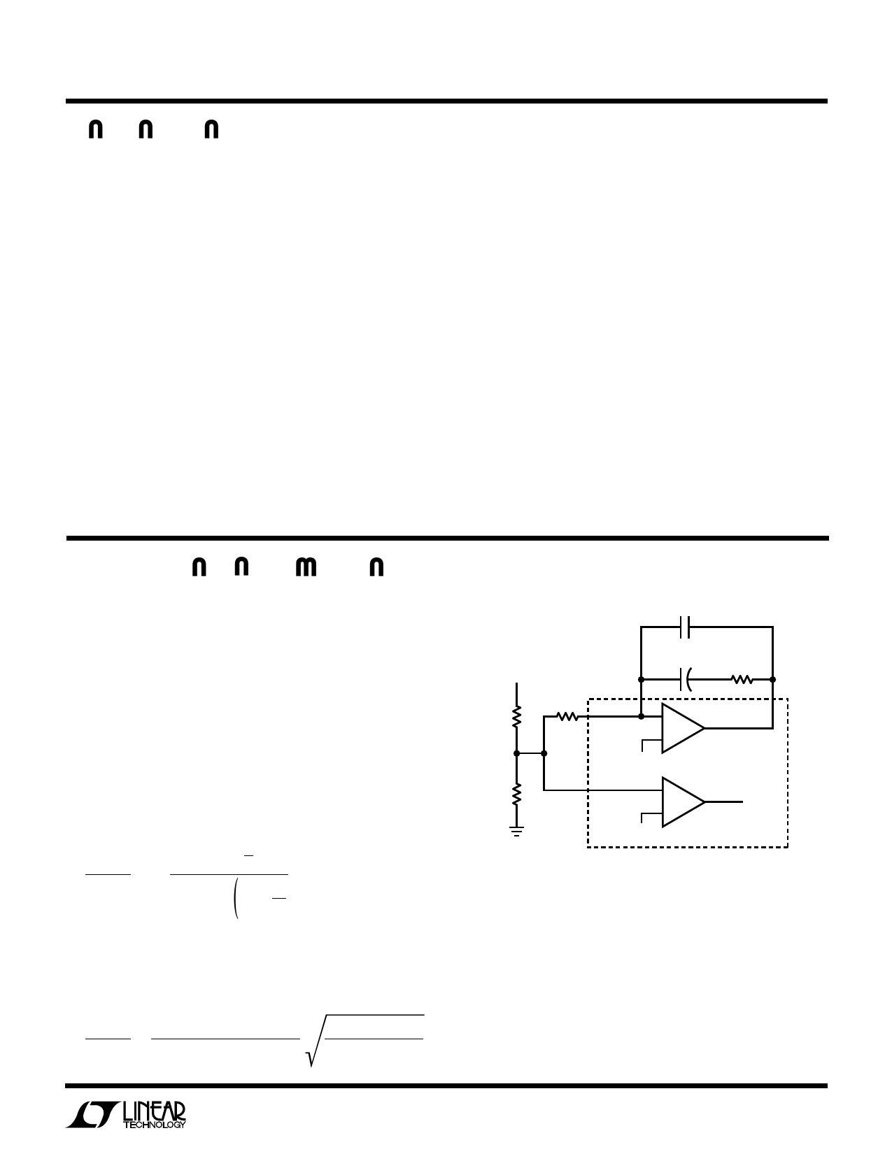
Voltage Error Amplifier (PFC Section)
The voltage error amplifier has a 100dB DC gain and 3MHz
unity-gain frequency. The output is internally clamped at
13.3V with VCC = 18V. Maximum error amp output voltage
decreases to VCC – 1.5V for VCC less than 12V. The
noninverting input is tied to the 7.5VREF through a diode
and can be pulled down with the SS1 pin. Referring to
Figure 1, VOUT = VREF [(R1 + R2)/R2]. With R1 = 1M and
R2 = 20k, VOUT = 382V. R1 through R4, C1 and C2 form the
compensation for the voltage loop. Gain of the voltage
error amp with the values shown is given by:
) VAOUT
VOUT
=
–
1
+
j
f
1
(j)(f)(6.6) 1 + j
f
11
The small-signal gain for the remaining portion of the
voltage loop for frequencies below the current loop band-
width is (see Figure 2):
VOUT =
VIN
VAOUT (5π)(j)(f)(COUT)(VOUT)
(RREF)(PIN)
RS(RIAC + 25k)
C2
0.047µF
REGULATOR OUTPUT
VOUT = 382V
R3
20k
R1
1M
R2
20k
C1
0.47µF
R4
330k
VSENSE
–
+
VREF = 7.5V
OVP
–
VAOUT
ERROR AMP
LT1509
+
1.05VREF
OVERVOLTAGE
COMPARATOR
LT1509 • F01
Figure 1
With VIN = 120VAC, PIN = 150W, RS = 0.15Ω, RREF = 4k,
RIAC = 1M, VOUT = 382V and COUT = 470µF, VOUT/VAOUT =
85/(j)(f). At very low frequencies, the loop has a – 40dB/
decade slope. Additional zero-pole compensation is added
at 1Hz and 11Hz. The resulting loop gain and phase margin
is shown in Figure 3. The unity-gain bandwidth is low
compared to 120Hz, which results in low distortion and a
high power factor.
7
Share Link: 