CXB1573R 데이터 시트보기 (PDF) - Sony Semiconductor
부품명
상세내역
일치하는 목록
CXB1573R Datasheet PDF : 21 Pages
| |||
CXB1573R
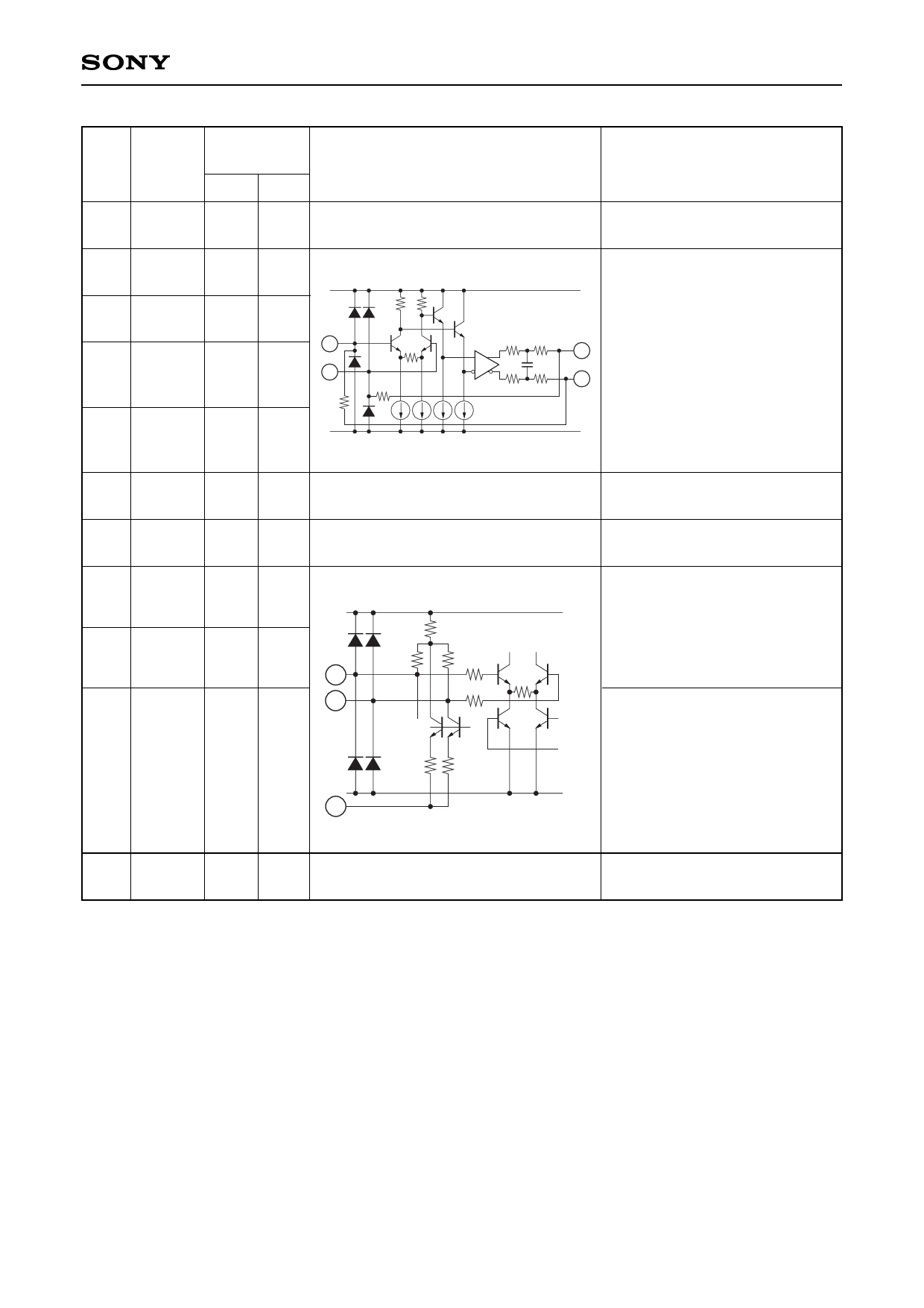
Typical pin
Pin
No.
Symbol voltage (V)
DC AC
10 VccY
3.3
11 CAP1B
12 CAP1
13 DB
14 D
15 VEE1
14
1.6
2
to
13
2.4
1k
1.6
2
to
2.4
0
16 VCC2
3.3
17 UP
18 DN
17
18
19 VEEl
0
19
20 VEE2
0
Equivalent circuit
Description
Positive power supply for analog
block.
VCC1
Pins 11 and 12 connect a
capacitor which determines the
7.5k 200
cut-off frequency for DC
12
100p
feedback block.
11 Pins 13 and 14 are input pins
1k
7.5k 200
for limiting amplifier block. Input
the signal with AC coupled.
VEE1
986
140.9
140.9
100
100
VCS
Negative power supply for analog
block.
Positive power supply for digital
block.
Connects a resistor for alarm
VCC2 level setting.
Default voltage can be generated
without an external resistor by
shorting the VEEI pin to VEE.
SW
SW
VEE2
Generates the default voltage
between UP and DOWN.
The voltage (8.0mV for input
conversion) can be generated
between UP and DOWN (Pins 17
and 18) as alarm setting level by
connecting this pin to VEE.
Negative power supply for digital
block.
–4–
Share Link: 