CXB1573R 데이터 시트보기 (PDF) - Sony Semiconductor
부품명
상세내역
일치하는 목록
CXB1573R Datasheet PDF : 21 Pages
| |||
CXB1573R
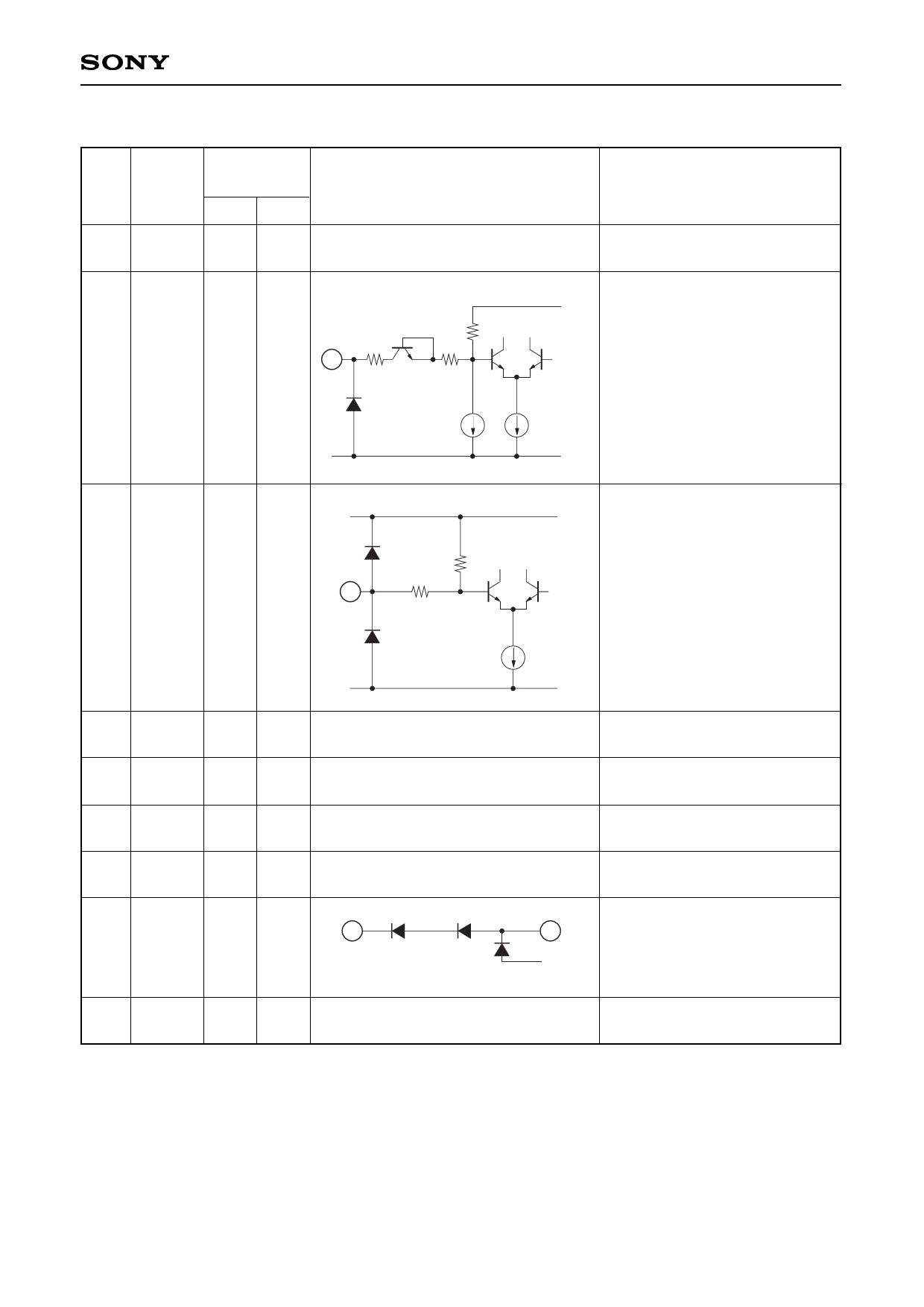
Pin Description
Typical pin
Pin
No.
Symbol voltage (V)
DC AC
1 VEE3
0
0
2 ODIS
or
3.3
(Open)
Equivalent circuit
Description
10k
2
300
10k
Negative power supply for ECL
output buffer.
VCC2
VREF
VEE2
Controls the output shutdown
function. High voltage when
open; the Q output is fixed to
Low. Low voltage when
connected to VEE; the D input
results in the Q output with ECL
level. TTL level is also available.
3 SW
0
or
3.3
(Open)
4 VCC2
3.3
5 VccX
3.3
6 VEE2
0
7 VEE1
0
8 TM
1.6
9 VCC1
3.3
60k
3
40k
7
VCC2
Switches the identification
maximum voltage amplitude.
High voltage when open; the
identification maximum voltage
amplitude becomes 40mVp-p.
Low voltage when connected to
VEE; the amplitude becomes
20mVp-p.
VEE2
Positive power supply for digital
block.
Positive power supply for digital
block.
Negative power supply for digital
block.
Negative power supply for analog
block.
8
Chip temperature monitor.
VEE1
Positive power supply for analog
block.
–3–
Share Link: 