P4C187 데이터 시트보기 (PDF) - Performance Semiconductor
부품명
상세내역
일치하는 목록
P4C187 Datasheet PDF : 8 Pages
| |||
P4C187/P4C187L
ULTRA HIGH SPEED 64K x 1
STATIC CMOS RAMS
FEATURES
Full CMOS, 6T Cell
High Speed (Equal Access and Cycle Times)
– 10/12/15/20/25 ns (Commercial)
– 12/15/20/25/35 ns (Industrial)
– 15/20/25/35/45 ns (Military)
Low Power Operation
– 743 mW Active -10
– 660/770 mW Active for -12/15
– 550/660 mW Active for -20/25/35
– 193/220 mW Standby (TTL Input)
– 83/110 mW Standby (CMOS Input) P4C187
– 5.5 mW Standby (CMOS Input) P4C187L (Military)
Single 5V±10% Power Supply
Data Retention with 2.0V Supply (P4C187L Military)
Separate Data I/O
Three-State Output
TTL Compatible Output
Fully TTL Compatible Inputs
Standard Pinout (JEDEC Approved)
– 22-Pin 300 mil DIP
– 24-Pin 300 mil SOJ
– 22-Pin 290x490 mil LCC
DESCRIPTION
The P4C187/L are 65, 536-bit ultra high speed static RAMs
organized as 64K x 1. The CMOS memories require no
clocks or refreshing and have equal access and cycle times.
The RAMs operate from a single 5V ± 10% tolerance power
supply. Data integrity is maintained for supply voltages down
to 2.0V, typically drawing 10µA.
Access times as fast as 10 nanoseconds are available,
greatly enhancing system speeds. CMOS reduces power
consumption to a low 743mW active, 193/83mW standby
for TTL/CMOS inputs and only 5.5 mW standby for the
P4C187L.
The P4C187/L are available in 22-pin 300 mil DIP, 24-pin
300 mil SOJ, and 22-pin LCC packages providing excellent
board level densities.
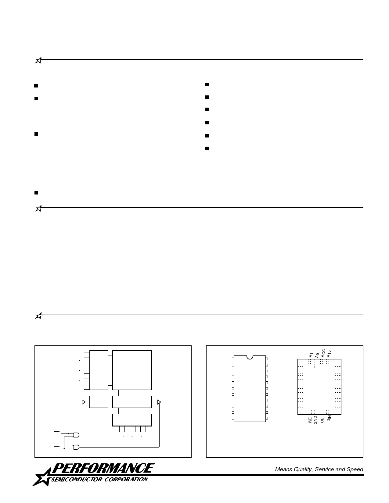
FUNCTIONAL BLOCK DIAGRAM
A
(8)
ROW
SELECT
65,356-BIT
MEMORY
ARRAY
A
DIN
INPUT
DATA
CONTROL
COLUMN I/O
COLUMN
SELECT
CE
A
A
(8)
WE
DOUT
PIN CONFIGURATIONS
A0 1
A1 2
A2 3
A3 4
A4 5
A5 6
A6 7
A7 8
DOUT 9
WE 10
GND 11
22 VCC
21 A15
20 A14
19 A13
18 A12
17 A11
16 A10
15 A9
14 A8
13 DIN
12 CE
A2
A3
A4
A5
A6
A7
DOUT
2
21
3
22 20
1
4
19
5
18
6
17
7
16
8
15
9
11 12 14
10
13
A14
A13
A12
A11
A10
A9
A8
DIP (P3, D3)
TOP VIEW
LCC (L3)
TOP VIEW
For SOJ pin configuration, please see Selection Guide.
Means Quality, Service and Speed
1Q97
55
Share Link: 