MJL16218 데이터 시트보기 (PDF) - Motorola => Freescale
부품명
상세내역
일치하는 목록
MJL16218 Datasheet PDF : 8 Pages
| |||
SAFE OPERATING AREA (continued)
MJL16218
FORWARD BIAS
There are two limitations on the power handling ability of a
transistor: average junction temperature and second break-
down. Safe operating area curves indicate IC – VCE limits of
the transistor that must be observed for reliable operation;
i.e., the transistor must not be subjected to greater dissipa-
tion than the curves indicate.
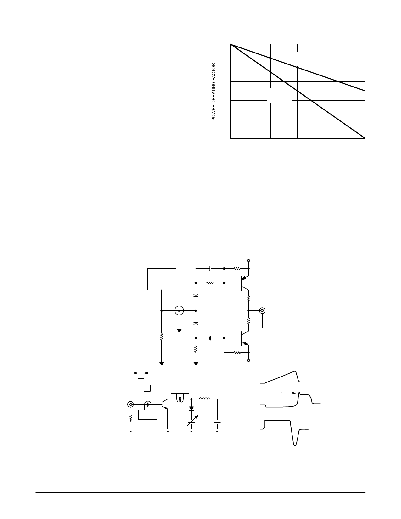
The data of Figure 1 is based on TC = 25_C; TJ(pk) is
variable depending on power level. Second breakdown pulse
limits are valid for duty cycles to 10% but must be derated
when TC ≥ 25_C. Second breakdown limitations do not
derate the same as thermal limitations. Allowable current at
the voltages shown on Figure 1 may be found at any case
temperature by using the appropriate curve on Figure 3.
At high case temperatures, thermal limitations will reduce
the power that can be handled to values less than the limita-
tions imposed by second breakdown.
REVERSE BIAS
For inductive loads, high voltage and high current must be
sustained simultaneously during turn–off, in most cases, with
the base–to–emitter junction reverse biased. Under these
conditions the collector voltage must be held to a safe level
at or below a specific value of collector current. This can be
accomplished by several means such as active clamping,
RC snubbing, load line shaping, etc.
1
0.8
0.6
0.4
0.2
0
25
SECOND BREAKDOWN
DERATING
THERMAL
DERATING
45
65
85
105
125
TC, CASE TEMPERATURE (°C)
Figure 3. Power Derating
The safe level for these devices is specified as Reverse
Biased Safe Operating Area and represents the voltage–
current condition allowable during reverse biased turnoff.
This rating is verified under clamped conditions so that the
device is never subjected to an avalanche mode. Figure 2
gives the RBSOA characteristics.
[ Lcoil (ICpk)
T1
VCC
T1 adjusted to obtain IC(pk)
V(BR)CEO
L = 10 mH
RB2 = ∞
VCC = 20 Volts
*Tektronix
*P–6042 or
*Equivalent
Table 1. RBSOA/V(BR)CEO(SUS) Test Circuit
0.02 µF
+ V ≈ 11 V
100
H.P. 214
OR EQUIV.
P.G.
0
20
+
– 10 µF
2N6191
RB1
≈ – 35 V
A
0.02 µF
RB2
50
+–
1 µF
500
2N5337
100
–V
T1
+V
0V
–V
*IC
L
IC
VCE(pk)
A
T.U.T.
MR856
VCE
50
*IB
Vclamp
VCC
IB
RBSOA
L = 200 µH
RB2 = 0
VCC = 20 Volts
RB1 selected for desired IB1
IC(pk)
IB1
IB2
Note: Adjust – V to obtain desired VBE(off) at Point A.
Motorola Bipolar Power Transistor Device Data
3
Share Link: 