MAX198ACAI-T 데이터 시트보기 (PDF) - Maxim Integrated
부품명
상세내역
일치하는 목록
MAX198ACAI-T Datasheet PDF : 16 Pages
| |||
Multirange, Single +5V, 12-Bit DAS
with 12-Bit Bus Interface
tCS
CS
tCSWS
WR
D7–D0
tWR
tDS
CONTROL
BYTE
ACQMOD = "1"
tCSHtAWCQI
tCONV
tDH
CONTROL
BYTE
ACQMOD = "0"
INT
tCSRS
tINT1
tCSRH
RD
DOUT
tD0
tTR
DATA VALID
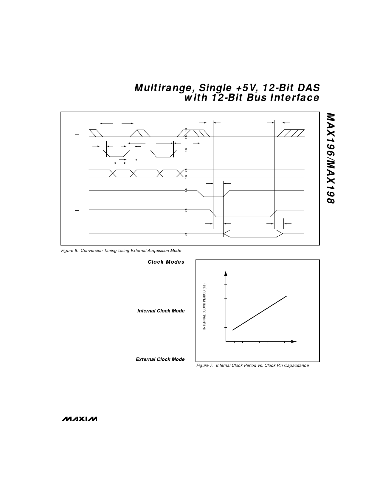
Figure 6. Conversion Timing Using External Acquisition Mode
Clock Modes
The MAX196/MAX198 operate with either an internal or
an external clock. Control bits (D6, D7) select either
internal or external clock mode. Once the desired clock
mode is selected, changing these bits to program
power-down will not affect the clock mode. In each
mode, internal or external acquisition can be used. At
power-up, external clock mode is selected.
Internal Clock Mode
Select internal clock mode to free the µP from the
burden of running the SAR conversion clock. To select
this mode, write the control byte with D7 = 0 and D6 =
1. A 100pF capacitor between the CLK pin and ground
sets this frequency to 1.56MHz nominal. Figure 7
shows a linear relationship between the internal clock
period and the value of the external capacitor used.
External Clock Mode
Select external clock mode by writing the control byte
with D7 = 0 and D6 = 0. Figure 8 shows CLK and WR
timing relationships in internal and external acquisition
modes, with an external clock. A 100kHz to 2.0MHz
external clock with 45% to 55% duty cycle is required for
proper operation. Operating at clock frequencies lower
than 100kHz will cause a voltage droop across the hold
capacitor, and subsequently degrade performance.
2000
1500
1000
500
0
0 50 100 150 200 250 300 350
CLOCK PIN CAPACITANCE (pF)
Figure 7. Internal Clock Period vs. Clock Pin Capacitance
______________________________________________________________________________________ 11
Share Link: 