A8740 데이터 시트보기 (PDF) - Allegro MicroSystems
부품명
상세내역
일치하는 목록
A8740
Allegro MicroSystems

A8740 Datasheet PDF : 18 Pages
| |||
A8740
Ultra Small Mobile Phone Xenon Photoflash
Capacitor Charger with IGBT Driver
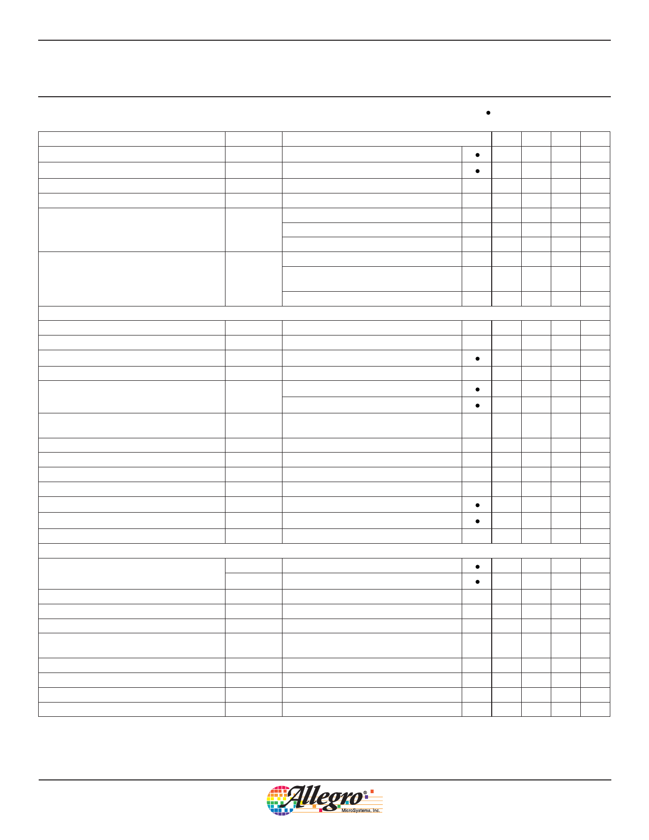
ELECTRICAL CHARACTERISTICS Typical values are valid at VIN = VBAT = 3.6 V; TA = 25°C, except
guaranteed from −40°C to 85°C ambient, unless otherwise noted
Characteristics
Symbol
Test Conditions
VBAT Voltage Range1
VIN_DRV Voltage Range1
UVLO Enable Threshold
UVLO Hysteresis
VBAT
VIN
VINUV
VINUV(hys)
VIN rising
Shutdown (CHARGE = 0 V, TRIG = 0 V)
VIN Supply Current
VBAT Pin Supply Current
IIN
Charging complete
Charging (CHARGE = VIN, TRIG = 0 V)
Shutdown (CHARGE = 0 V, TRIG = 0 V)
IBAT
Charging done (CHARGE = VIN,
¯D¯¯O¯¯N¯¯E¯ = 0 V)
Current Limit
Charging (CHARGE = VIN, TRIG = 0 V)
Primary-Side Current Limit2
Switch On-Resistance
Switch Leakage Current1
CHARGE Pull-down Resistance
CHARGE Input Voltage1
ISWLIM
RSWDS(on)
ISWLK
RCHGPD
VCHARGE
VIN_DRV = 3.6 V, ID = 600 mA, TA = 25°C
VSW = 5.5, over full temperature range
High, over input supply range
Low, over input supply range
CHARGE On/Off Delay
tCH
Time between CHARGE = 1 and charging
enabled
Switch-Off Timeout
Switch-On Timeout
Output Comparator Trip Voltage3
Output Comparator Voltage Overdrive
¯D¯¯O¯¯N¯¯E¯ Output Leakage Current1
¯D¯¯O¯¯N¯¯E¯ Output Low Voltage1
dV/dt Threshold for ZVS Comparator
toff(max)
ton(max)
VOUTTRIP
VOUTOV
IDONELK
VDONEL
dV/dt
Measured as VSW – VBAT
Pulse width = 200 ns (90% to 90%)
32 μA into ¯D¯¯O¯¯N¯¯E¯ pin
Measured at SW pin
IGBT Driver
TRIG Input Voltage1
VTRIG(H)
VTRIG(L)
Input = logic high, over input supply range
Input = logic low, over input supply range
TRIG Pull-Down Resistor
RTRIGPD
GATE Resistance to VIN_DRV
RSrcDS(on) VGATE = 1.8 V
GATE Resistance to GND
Propagation Delay (Rising)4,5
RSnkDS(on)
tDr
VGATE = 1.8 V
Measurement taken at ¯D¯¯O¯¯N¯¯E¯ pin,
CL= 6500 pF
Propagation Delay (Falling)4,5
tDf
Output Rise Time4,5
tr
Output Fall Time4,5
tf
GATE Pull-Down Resistor
RGTPD
1Specifications throughout the range TA = –40°C to 85°C guaranteed by design and characterization.
2Current limit guaranteed by design and correlation to static test.
3Specifications throughout the range TA = –20°C to 85°C guaranteed by design and characterization.
4Guaranteed by design and characterization.
5See IGBT Drive Timing Definition diagram for further information.
indicates specifications
Min. Typ. Max. Unit
1.5 – 5.5 V
2.3 – 5.5 V
– 2.05 2.2 V
– 150 – mV
– 0.02 0.5 μA
–
50 100 μA
–
2
– mA
– 0.01 1
μA
–
–
5
μA
–
–
50 μA
1.35 1.5 1.65 A
– 0.4 –
Ω
–
–
2
μA
– 130 –
kΩ
1.3 –
–
V
–
– 0.5 V
–
20
–
us
–
18
–
μs
–
18
–
μs
31.0 31.5 32.0 V
– 200 400 mV
–
–
1
μA
–
– 100 mV
–
20
– V/μs
1.3 –
–
V
–
– 0.5 V
– 130 –
kΩ
– 6.6 –
Ω
–
50
–
Ω
–
25
–
ns
–
60
–
ns
–
80
–
ns
– 700 –
ns
–
20
–
kΩ
Allegro MicroSystems, Inc.
4
115 Northeast Cutoff
Worcester, Massachusetts 01615-0036 U.S.A.
1.508.853.5000; www.allegromicro.com
Share Link: