A8438(2005) 데이터 시트보기 (PDF) - Allegro MicroSystems
부품명
상세내역
일치하는 목록
A8438 Datasheet PDF : 13 Pages
| |||
A8438 Photoflash Capacitor Charger with IGBT Driver
Applications Information
Transformer Design
Turns Ratio. The minimum transformer turns ratio, N,
(Secondary:Primary) should be chosen based on the following
formula:
N ≥ VOUT + VD_Drop
(2)
40 − VBATT
where:
VOUT (V) is the required output voltage level,
VD_Drop (V) is the forward voltage drop of the output diode(s),
VBATT (V) is the transformer battery supply, and
40 (V) is the rated voltage for the internal MOSFET switch,
representing the maximum allowable reflected voltage from the
output to the SW pin.
For example, if VBATT is 3.5 V and VD_Drop is 1.7 V (which could
be the case when two high voltage diodes were in series), and the
desired VOUT is 320 V, then the turns ratio should be at least 8.9.
In a worst case, when VBATT is highest and VD_Drop and VOUT are
at their maximum tolerance limit, N will be higher. Taking VBATT
= 5.5 V, VD_Drop = 2 V, and VOUT = 320 V × 102 % = 326.4 V as
the worst case condition, N can be determined to be 9.5.
In practice, always choose a turns ratio that is higher than the
calculated value to give some safety margin. In the worst case
example, a minimum turns ratio of N = 10 is recommended.
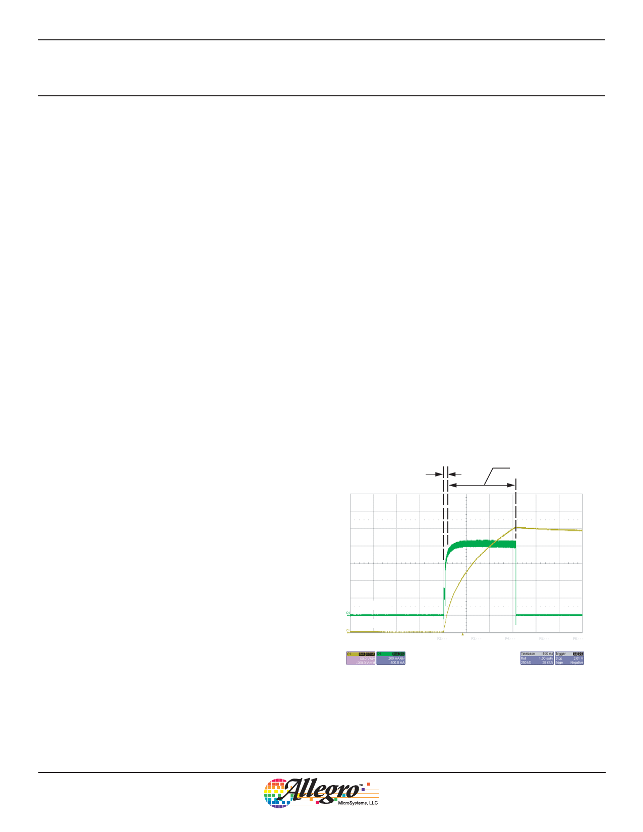
Primary Inductance. The A8438 has a minimum switch off-time,
tOFF(min) , of 300 ns, to ensure correct SW node voltage sensing.
As a loose guideline when choosing the primary inductance,
LPrimary (μH), use the following formula:
LPrimary
≥
300 ×10−9 ×VOUT
N × ISWLIM
.
(3)
Ideally, the charging time is not affected by transformer primary
inductance. In practice, however, it is recommended that a
primary inductance be chosen between 10 μH and 20 μH. When
LPrimary is less than 10 μH, parasitic elements associated with
flyback from the transformer lead to lower efficiency and longer
charging time. When LPrimary is greater than 20 μH, the rating
of the transformer must be dramatically increased to handle the
required power density, and the series resistances are usually
higher. A design that is optimized to achieve a small footprint
solution would have an LPrimary of 12 to 14 μH, with minimized
leakage inductance and secondary capacitance, and minimized
primary and secondary series resistance. Please refer to the table
Recommended Components for more information.
Leakage Inductance and Secondary Capacitance. The trans-
former design should minimize the leakage inductance to ensure
the turn-off voltage spike at the SW node does not exceed the
40 V limit. An achievable minimum leakage inductance for this
application, however, is usually compromised by an increase in
parasitic capacitance. Furthermore, the transformer secondary
capacitance should be minimized. Any secondary capacitance is
multiplied by N2 when reflected to the primary, leading to high
initial current swings when the switch turns on, and to reduced
efficiency.
VBIAS 3.0 to 5.5 V
Two Alkaline/NiMH/NiCAD or one Li +
VBATT 1.5 to 5.5 V
T1
D1
VOUT
R5
100 kΩ
R4
10 kΩ
C1
0.1 μF
C2
4.7 μF
VIN
ILIM
CHARGE
DONE
SW
FB
A8436
TRIGGER
IGBTDRV
GND
To IGBT Gate
R1
150 kΩ
R2
150 kΩ
R3
1.2 kΩ
COUT
303 V
Figure 6. Typical circuit for photoflash application. Configured for ISWLIM of 2.0 A.
A8438-DS, Rev. 1
Symbol
C1
C2
D1
T1
R1, R2
R3
R4, R5
Rating
0.1 μF, X5R or X7R, 10 V
4.7 μF, X5R or X7R, 10 V
Fairchild Semiconductor BAV23S
(dual diode connected in series)
TDK LDT565630T-041,
LPrimary = 4.7 μH, N = 10.2
1206 Resistor, 1 %
0603 Resistor, 1 %
Pull-up resistors
Allegro MicroSystems, Inc.
11
115 Northeast Cutoff, Box 15036
Worcester, Massachusetts 01615-0036 (508) 853-5000
www.allegromicro.com
Share Link: 