BR24T16FVJ-W 데이터 시트보기 (PDF) - ROHM Semiconductor
부품명
상세내역
일치하는 목록
BR24T16FVJ-W Datasheet PDF : 39 Pages
| |||
BR24T16-W
Datasheet
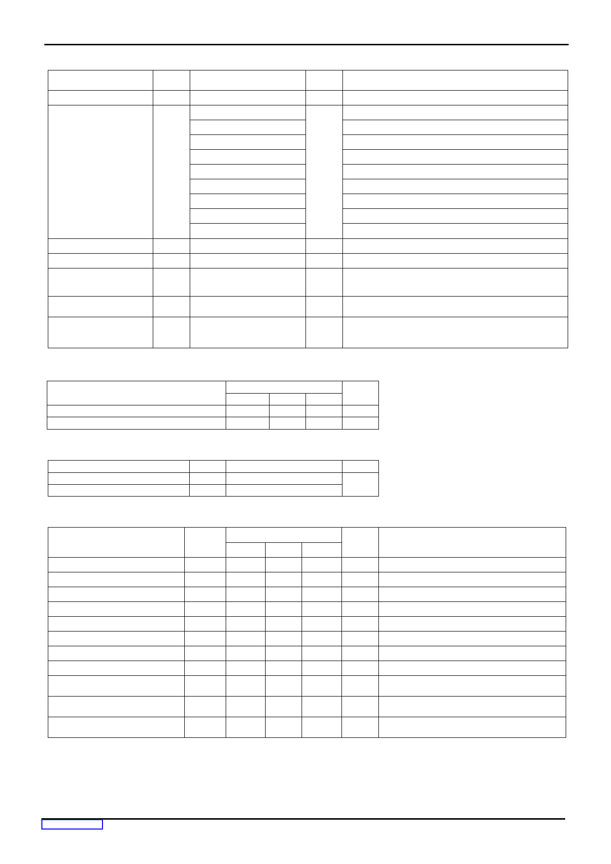
Absolute Maximum Ratings (Ta=25ºC)
Parameter
Symbol
Rating
Supply Voltage
VCC
Power Dissipation
Pd
Storage Temperature
Tstg
Operating Temperature Topr
-0.3 to +6.5
450 (SOP8)
450 (SOP-J8)
450 (SOP-J8A)
300 (SSOP-B8)
330 (TSSOP-B8)
310 (TSSOP-B8J)
310 (MSOP8)
300 (VSON008X2030)
800 (DIP-T8)
-65 to +150
-40 to +85
Input Voltage /
Output Voltage
Junction
Temperature
Electrostatic discharge
voltage
(human body model)
‐
Tjmax
VESD
-0.3 to Vcc+1.0
150
-4000 to +4000
Unit
Remark
V
Derate by 4.5mW/°C when operating above Ta=25°C
Derate by 4.5mW/°C when operating above Ta=25°C
Derate by 4.5mW/°C when operating above Ta=25°C
mW
Derate by 3.0mW/°C when operating above Ta=25°C
Derate by 3.3mW/°C when operating above Ta=25°C
Derate by 3.1mW/°C when operating above Ta=25°C
Derate by 3.1mW/°C when operating above Ta=25°C
Derate by 3.0mW/°C when operating above Ta=25°C
Derate by 8.0mW/°C when operating above Ta=25°C
°C
°C
The Max value of input voltage / output voltage is not over 6.5V.
V
When the pulse width is 50ns or less, the Min value of input voltage
/ output voltage is not lower than -1.0V.
°C Junction temperature at the storage condition
V
Memory Cell Characteristics (Ta=25ºC, Vcc=1.6V to 5.5V)
Parameter
Limit
Min
Typ Max
Write Cycles (1)
1,000,000 -
-
Data Retention (1)
40
-
-
(1) Not 100% TESTED
Unit
Times
Years
Recommended Operating Ratings
Parameter
Symbol
Rating
Unit
Power Source Voltage
Input Voltage
Vcc
1.6 to 5.5
VIN
0 to Vcc
V
DC Characteristics (Unless otherwise specified, Ta=-40ºC to +85ºC, Vcc=1.6V to 5.5V)
Parameter
Limit
Symbol
Unit
Min Typ Max
Conditions
Input High Voltage1
VIH1 0.7Vcc - Vcc+1.0 V 1.7V≦Vcc≦5.5V
Input Low Voltage1
VIL1
-0.3(2)
- +0.3Vcc V 1.7V≦Vcc≦5.5V
Input High Voltage2
VIH2 0.8Vcc - Vcc+1.0 V 1.6V≦Vcc<1.7V
Input Low Voltage2
VIL2
-0.3(2)
- +0.2Vcc V 1.6V≦Vcc<1.7V
Output Low Voltage1
VOL1
-
-
0.4
V IOL=3.0mA, 2.5V≦Vcc≦5.5V (SDA)
Output Low Voltage2
VOL2
-
-
0.2
V IOL=0.7mA, 1.6V≦Vcc<2.5V (SDA)
Input Leakage Current
ILI
-1
-
1
µA VIN=0 to Vcc
Output Leakage Current
Supply Current (Write)
ILO
-1
ICC1
-
Supply Current (Read)
ICC2
-
Standby Current
ISB
-
(2) When the pulse width is 50ns or less, it is -1.0V.
-
1
µA VOUT=0 to Vcc (SDA)
-
2.0
mA
Vcc=5.5V, fSCL=400kHz, tWR=5ms,
Byte write, Page write
-
0.5
mA
Vcc=5.5V, fSCL=400kHz
Random read, current read, sequential read
-
2.0
µA
Vcc=5.5V, SDA・SCL=Vcc
A0,A1,A2=GND,WP=GND
www.rohm.com
©2013 ROHM Co., Ltd. All rights reserved.
TSZ22111・15・001
2/35
TSZ02201-0R2R0G100110-1-2
30.Aug.2017 Rev.006
Share Link: 