IR2121 데이터 시트보기 (PDF) - Infineon Technologies
부품명
상세내역
일치하는 목록
IR2121 Datasheet PDF : 16 Pages
| |||
IR2121 & (PbF)
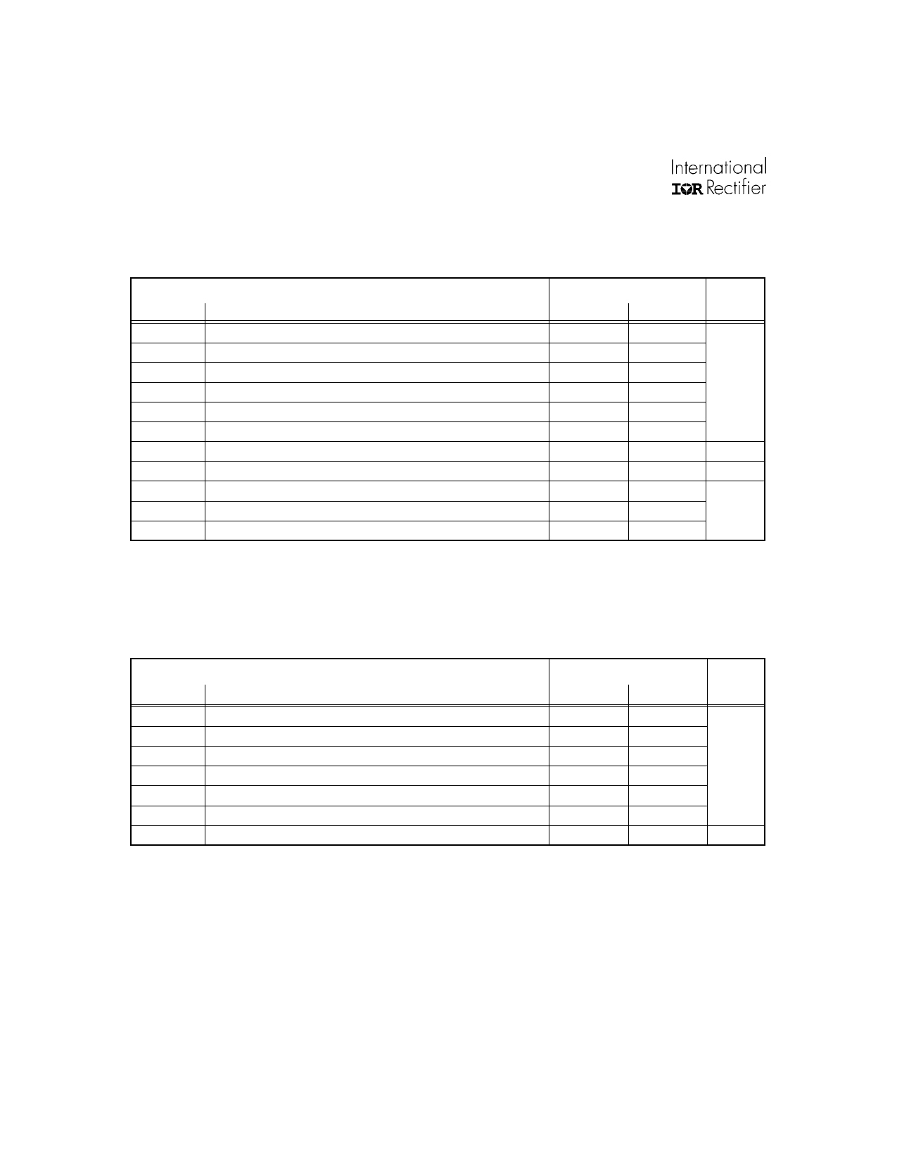
Absolute Maximum Ratings
Absolute Maximum Ratings indicate sustained limits beyond which damage to the device may occur. All voltage param-
eters are absolute voltages referenced to COM. The Thermal Resistance and Power Dissipation ratings are measured
under board mounted and still air conditions.
Parameter
Value
Symbol
Definition
Min.
Max. Units
VCC
VS
VO
VIN
VERR
VCS
PD
RthJA
TJ
TS
TL
Fixed Supply Voltage
Gate Drive Return Voltage
Output Voltage
Logic Input Voltage
Error Signal Voltage
Current Sense Voltage
Package Power Dissipation @ TA ≤ +25°C
Thermal Resistance, Junction to Ambient
Junction Temperature
Storage Temperature
Lead Temperature (Soldering, 10 seconds)
-0.3
VCC - 25
VS - 0.3
-0.3
-0.3
VS - 0.3
—
—
—
-55
—
25
VCC + 0.3
VCC + 0.3
VCC + 0.3
VCC + 0.3
VCC + 0.3
1.0
125
150
150
300
V
W
°C/W
°C
Recommended Operating Conditions
The Input/Output logic timing diagram is shown in Figure 1. For proper operation the device should be used within the
recommended conditions. The VS offset rating is tested with all supplies biased at 15V differential.
Symbol
VCC
VS
VO
VIN
VERR
VCS
TA
Parameter
Definition
Fixed Supply Voltage
Gate Drive Return Voltage
Output Voltage
Logic Input Voltage
Error Signal Voltage
Current Sense Signal Voltage
Ambient Temperature
Value
Min.
Max.
VS + 12
-5
VS + 18
5
VS
VCC
0
VCC
0
VCC
VS
VCC
-40
125
Units
V
°C
2
www.irf.com
Share Link: 