IDT74163244PF 데이터 시트보기 (PDF) - Integrated Device Technology
부품명
상세내역
일치하는 목록
IDT74163244PF Datasheet PDF : 6 Pages
| |||
IDT74FST163244
16-BIT BUS SWITCH
COMMERCIAL TEMPERATURE RANGE
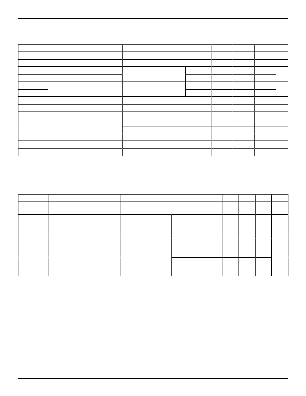
DC ELECTRICAL CHARACTERISTICS OVER OPERATING RANGE
Following Conditions Apply Unless Otherwise Specified:
Commercial: TA = –40°C to +85°C, VCC = 5.0V ±10%
Symbol
VIH
Parameter
Input HIGH Voltage
Test Conditions(1)
Guaranteed Logic HIGH for Control Inputs
Min.
2.0
Typ.(2)
—
Max. Unit
—
V
VIL
Input LOW Voltage
Guaranteed Logic LOW for Control Inputs
—
—
0.8
V
II H
Input HIGH Current
VCC = Max.
VI = VCC
—
—
±1
µA
II L
Input LOW Voltage
VI = GND
—
—
±1
IOZH
High Impedance Output Current VCC = Max.
VO = VCC
—
—
±1
µA
IOZL
(3-State Output pins)
IOS
Short Circuit Current
VO = GND —
—
±1
VCC = Max., VO = GND(3)
—
300
— mA
VIK
Clamp Diode Voltage
RON
Switch On Resistance(4)
VCC = Min., IIN = –18mA
VCC = Min., VIN = 0.0V
ION = 12mA
—
–0.7
–1.2 V
—
5
7
Ω
VCC = Min., VIN = 2.4V
—
10
15
Ω
ION = 8mA
IOFF
Input/Output Power Off Leakage VCC = 0V, VIN or VO ≤ 4.5V
—
—
±1
µA
ICC
Quiescent Power Supply Current VCC = Max., VIN = GND or VCC
—
0.1
3
NOTES:
1. For conditions shown as Max. or Min., use appropriate value specified under Electrical Characteristics for the applicable device type.
2. Typical values are at VCC = 5.0V, +25°C ambient.
3. Not more than one output should be tested at one time. Duration of the test should not exceed one second.
4. Measured by voltage drop between ports at indicated current through the switch.
µA
3615 tbl 05
POWER SUPPLY CHARACTERISTICS
Symbol
Parameter
Test Conditions(1)
Min. Typ.(2) Max.
∆ICC
Quiescent Power Supply Current VCC = Max.
TTL Inputs HIGH
VIN = 3.4V(3)
— 0.5 1.5
ICCD
IC
Dynamic Power Supply
Current(4)
Total Power Supply Current(6)
VCC = Max.
VIN = VCC
Outputs Open
VIN = GND
Enable Pin Toggling
50% Duty Cycle
VCC = Max.
VIN = VCC
Outputs Open
VIN = GND
4 Enable Pins Toggling
—
30
40
— 4.8 6.4
(16 Switches Toggling) VIN = 3.4
fi = 10MHz
VIN = GND
50% Duty Cycle
— 5.3 7.9
NOTES:
1. For conditions shown as Max. or Min., use appropriate value specified under Electrical Characteristics for the applicable device type.
2. Typical values are at VCC = 5.0V, +25°C ambient.
3. Per TTL driven input (VIN = 3.4V). All other inputs at VCC or GND.
4. This parameter is not directly testable, but is derived for use in Total Power Supply Calculations.
5. Values for these conditions are examples of the ICC formula. These limits are guaranteed but not tested.
6. IC = IQUIESCENT + IINPUTS + IDYNAMIC
IC = ICC + ∆ICC DHNT + ICCD (fiN)
ICC = Quiescent Current
∆ICC = Power Supply Current for a TTL High Input (VIN = 3.4V)
DH = Duty Cycle for TTL Inputs High
NT = Number of TTL Inputs at DH
ICCD = Dynamic Current Caused by an Input Transition Pair (HLH or LHL)
fi = Input Frequency
N = Number of Switches Toggling at fi
All currents are in milliamps and all frequencies are in megahertz.
Unit
mA
µA/
MHz/
Switch
mA
3615 tbl 06
3
Share Link: 