ICS9248F-169-T 데이터 시트보기 (PDF) - Integrated Circuit Systems
부품명
상세내역
일치하는 목록
ICS9248F-169-T
Integrated Circuit Systems

ICS9248F-169-T Datasheet PDF : 14 Pages
| |||
ICS9248-169
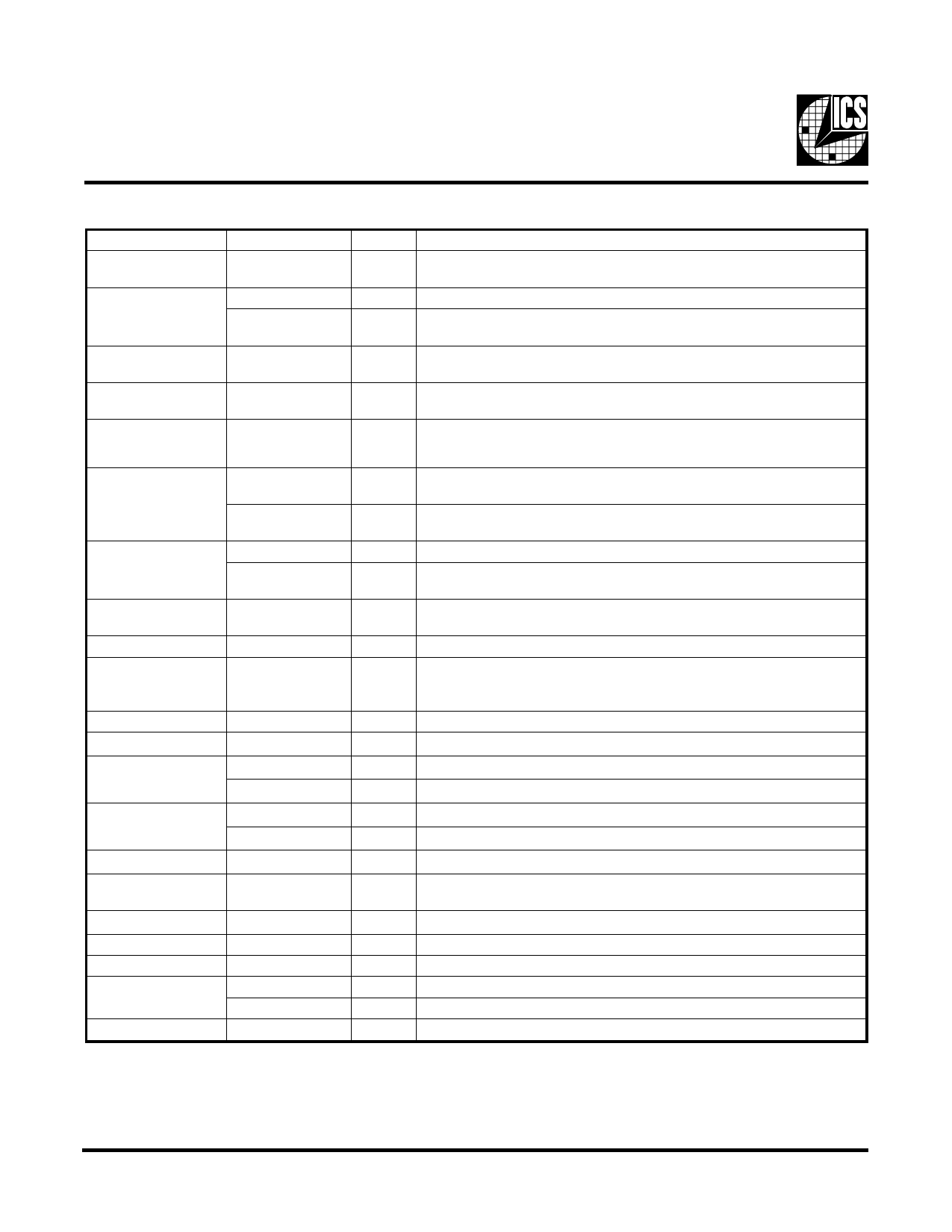
Pin Descriptions
PIN NUMBER
1, 6, 14, 19,
27, 30, 36
2
3,9,16,22,
33,39,45
4
PIN NAME
VDD
REF0
PCI_STOP#1
GND
X1
5
X2
PCICLK_F
7
MODE1, 2
FS3
8
PCICLK0
13, 12, 11, 10
15
17, 18, 20, 21,
28, 29, 31, 32,
34, 35,37,38
23
24
25
26
40
41
42, 48
43
44
46
47
PCICLK (4:1)
BUFFER IN
SDRAM (11:0)
SDATA
SCLK
24MHz
FS11, 2
48MHz
FS01, 2
SDRAM_F
CLK_STOP#
VDDL
CPUCLK1
CPUCLK_F
REF1
FS21, 2
IOAPIC
TYPE
DESCRIPTION
PWR 3.3V Power supply
OUT 14.318 Mhz reference clock.
IN
Halts PCICLK(0:4) clocks at logic 0 level, when input low (In
mobile mode, MODE=0)
PWR Ground
IN
OUT
OUT
IN
IN
OUT
OUT
IN
Crystal input, has internal load cap (36pF) and feedback
resistor from X2
Crystal output, nominally 14.318MHz. Has internal load
cap (36pF)
Free running PCI clock not affected by PCI_STOP# for power
management.
Pin 7 function select pin, 1=Desktop Mode, 0=Mobile Mode.
Latched Input.
Frequency select pin. Latched Input. Internal Pull-down to GND
PCI clock outputs. Syncheronous to CPU clocks with 1-4ns skew
(CPU early)
PCI clock outputs. Syncheronous to CPU clocks with 1-4ns skew
(CPU early)
Input to Fanout Buffers for SDRAM outputs.
OUT
SDRAM clock outputs, Fanout Buffer outputs from BUFFER IN pin
(controlled by chipset).
I/O
IN
OUT
IN
OUT
IN
OUT
IN
PWR
OUT
OUT
OUT
IN
OUT
Data pin for I2C circuitry 5V tolerant
Clock pin of I2C circuitry 5V tolerant
24MHz output clock
Frequency select pin. Latched Input.
48MHz output clock
Frequency select pin. Latched Input
Free running SDRAM clock output. Not affected by CPU_STOP#
This asynchronous input halts CPUCLK1, IOAPIC & SDRAM
(0:11) at logic "0" level when driven low.
Supply for CPU, IOAPIC clocks, either 2.5V or 3.3V nominal
CPU clock outputs, powered by VDDL2. Low if CPU_STOP#=Low
Free running CPU clock. Not affected by the CPU_STOP#
14.318 MHz reference clock.
Frequency select pin. Latched Input
IOAPIC clock output. 14.318 MHz Powered by VDDL1.
Notes:
1: Internal Pull-up Resistor of 120K to 3.3V on indicated inputs
2: Bidirectional input/output pins, input logic levels are latched at internal power-on-reset. Use 10Kohm resistor
to program logic Hi to VDD or GND for logic low.
Third party brands and names are the property of their respective owners.
2
Share Link: