AV9248F-77 데이터 시트보기 (PDF) - Integrated Circuit Systems
부품명
상세내역
일치하는 목록
AV9248F-77 Datasheet PDF : 14 Pages
| |||
ICS9248-77
Power Groups:
VDDREF, GNDREF = REF, X1, X2
GNDPCI, VDDPCI = PCICLK
VDD66, GND66 = 3V66
VDD48, GND48 = 48MHz
VDDCOR, GNDCOR = PLL Core
VDDLCPU/2 , GNDLCPU/2 = CPU/2
VDDLIOAPIC, GNDIOAPIC = IOAPIC
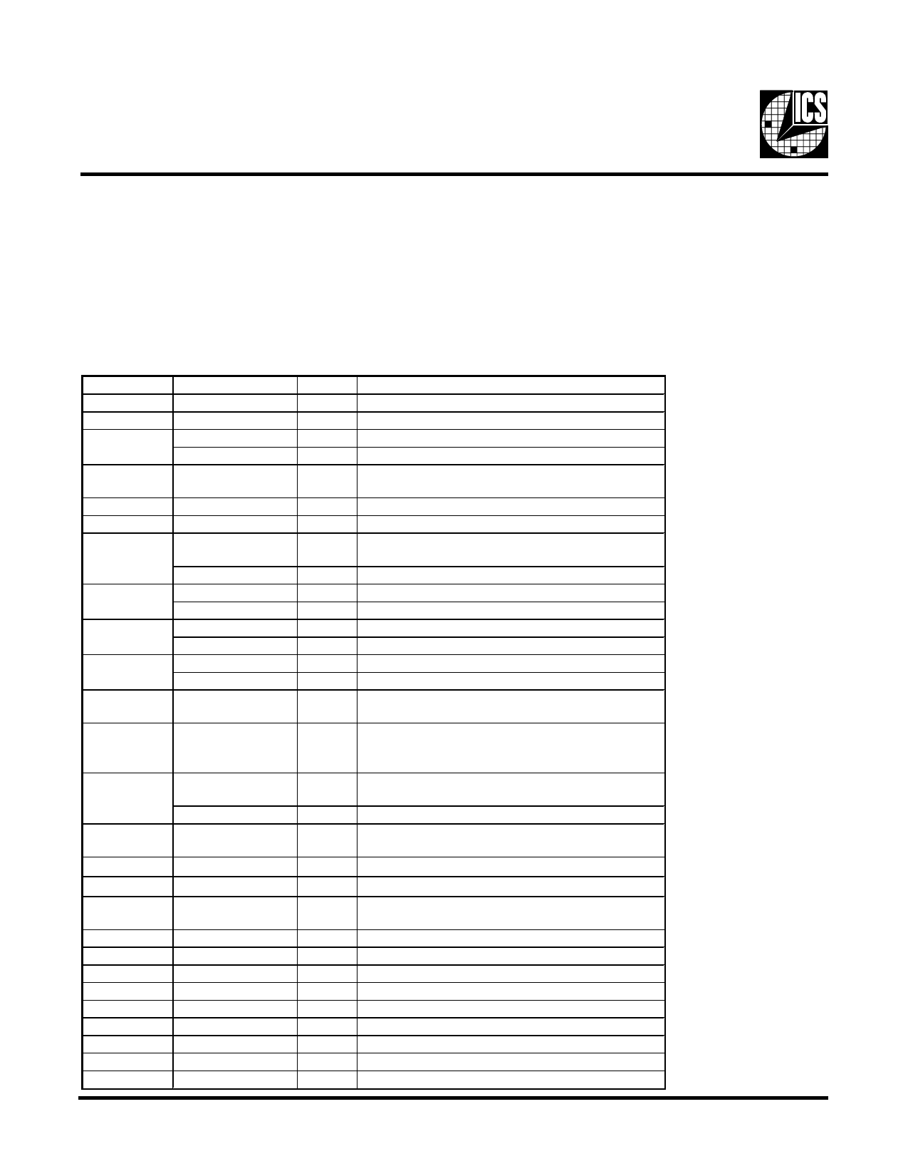
Pin Descriptions
Pin number
Pin name
1, 7, 13, 19, 25, 31 GND
2
REF0
3
REF1
SEL24_48
4, 10, 16, 23,
28, 35
VDD
5
X1
6
X2
8
PCICLK_F
FS0
PCICLK1
9
FS1
11
PCICLK2
FS2
PCICLK3
12
FS3
14, 15, 17, 18, 20,
PCICLK [4:10]
21, 22
24
PD#
26
27
29
30
32, 33, 34
36
37, 38, 40
39
41
42
43
45
44, 46, 47
48
24_48MHz
FREQ_APIC
48MHz/SEL_3V66
SCLK
SDATA
3V66[0:2]
GNDLCPU
CPUCLK[0:2]
VDDLCPU
GNDLCPU/2
CPU/2
VDDLCPU/2
GNDLIOAPIC
IOAPIC[0:2]
VDDLIOAPIC
Type
PWR
OUT
OUT
IN
Description
Ground pins
14.318MHz reference clock outputs at 3.3V
14.318MHz reference clock outputs at 3.3V
Logic input to select 24 or 48MHz for pin 26 output
PWR Power pins 3.3V
IN XTAL_IN 14.318MHz crystal input
OUT XTAL_OUT Crystal output
Free running PCI clock at 3.3V. Synchronous to CPU clocks. Not
OUT affected by the PCI_STOP# input.
IN Logic - input for frequency selection
OUT PCI clock output at 3.3V. Synchronous to CPU clocks.
IN Logic - input for frequency selection
OUT PCI clock output at 3.3V. Synchronous to CPU clocks.
IN Logic - input for frequency selection
OUT PCI clock output at 3.3V. Synchronous to CPU clocks.
IN Logic - input for frequency selection
OUT PCI clock outputs at 3.3V. Synchronous to CPU clocks.
IN
OUT
IN
OUT/IN
IN
IN
OUT
PWR
OUT
PWR
PWR
OUT
PWR
PWR
OUT
PWR
This asynchronous input powers down the chip when drive
active(Low). The internal PLLs are disabled and all the output clocks
are held at a Low state.
24 or 48MHz output selectable by
SEL24_48# (0=48MHz 1=24MHz)
Logic input for frequency selection of IOAPIC
Fixed 48MHz clock output. 3.3V / Logic input to select the
frequency of the 3V66 outputs
Clock input of I2C input
Data input for I2C serial input.
3.3V clock outputs. These outputs are stopped when CPU_STOP#
is driven active..
Ground pin for the CPUCLKs
Host bus clock output at 2.5V.
Power pin for the CPUCLKs. 2.5V
Ground pin for the CPU/2 clocks.
2.5V clock outputs at 1/2 CPU frequency.
Power pin for the CPU/2 clocks. 2.5V
Ground pin for the IOAPIC outputs.
IOAPIC clocks at 2.5V. Synchronous with CPUCLKs
Power pin for the IOAPIC outputs. 2.5V.
2
Share Link: 